


– 41 –
•
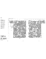
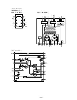
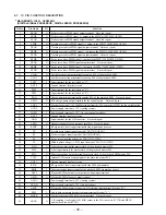
MAIN BOARD IC701 MSM65354-412GS-BK4 (SYSTEM CONTROLLER, LCD DRIVER, KEY CONTROL)
Pin No.
Pin Name
I/O
Function
1 to 4
COM1 to COM4
O
Common drive signal output to the liquid crystal display (LCD401)
5 to 11
SEG0 to SEG6
O
Segment drive signal output to the liquid crystal display (LCD401)
12
NC
O
Not used (open)
13 to 18
SEG7 to SEG12
O
Segment drive signal output to the liquid crystal display (LCD401)
19 to 36
NC
O
Not used (open)
37
AGND
—
Ground terminal (analog system)
38
DC CHK
I
DC in voltage detection input terminal (A/D input) Also used for DC IN detection
39
DOOR OPEN
I
CD lid open/close detection switch (S401) input terminal
The stop status is reset with the falling edge of input signal
“H”: CD lid open, “L”: CD lid close
40
KEY IN1
I
Key input terminal (A/D input)
RETURN, MENU –, PREV
=
,
^
, NEXT
+
, MENU + keys input (S441 to S446)
41
KEY IN2
I
Key input terminal (A/D input)
p
POWER OFF, SELECT keys input (S421 and S422)
42
BATT CHK
I
Battery voltage detection input terminal
43
NTSC/PAL
I
Video system select switch (S703) input terminal “L”: NTSC, “H”: AUTO
44
DCINJACK
I
DC IN 6V jack (J801) detection input terminal “L”: plug in
45
MODE
I
Fixed at “L” in this set
46
VRH
I
Reference voltage input terminal (+3.3V) (for A/D converter)
47
AVDD
—
Power supply terminal (+3.3V) (analog system)
48
DBB CTL1
O
MEGA BASS on/off control signal output terminal
“L”: MEGA BASS on (level-1 and level-2) Not used (open)
49
AU-MUTE
O
Analog line mute control signal output terminal “H”: mute on
50
XAU-RESET
O
Reset signal output to the CXD2545Q (IC601) and headphone amplifier (IC360) “L”: reset
51
XV-RESET
O
Reset signal output to the MPEG audio/video decoder (IC901) and video encoder (IC920)
“L”: reset
52
HOLD
I
HOLD switch (S701) input terminal “L”: hold off, “H”: hold on
53
RESUME
I
RESUME switch (S702) input terminal “L”: resume off, “H”: resume on
54
XDSPLT
O
Serial data latch pulse signal output to the CXD2545Q (IC601)
55
XDACLT
O
Serial data latch pulse signal output to the D/A converter (IC320)
56
V-POWER
O
Video CD system power supply on/off control signal output terminal “L”: power on
57
AU-POWER
O
Audio CD system power supply on/off control signal output terminal “L”: power on
58
ESP-POWER
O
Control signal output to the ESP (Electronic Shock Protection) circuit
59
TRVCTL
O
Tracking gain control signal output terminal
60 to 63
TRV3 to TRV0
O
Tracking balance control signal output terminal
64
XSOE
O
Serial data output enable signal output terminal Not used (open)
65
DSP-SUBQ
I
Sub-code Q data signal input from the CXD2545Q (IC601)
66
DSP-SBQCLK
O
Sub-code Q data reading clock signal output to the CXD2545Q (IC601)
67
REMOTE
I
Sircs remote control signal input from the remote control receiver (IC401)
68
DSP-DATA
O
Serial data output to the CXD2545Q (IC601) and D/A converter (IC320)
69
DSP-SENS
I
Internal status (SENSE) signal input from the CXD2545Q (IC601)
70
DSP-CLK
O
Serial data transfer clock signal output to the CXD2545Q (IC601) and D/A converter (IC320)
71
DSP-SNSCLK
O
Sense serial data reading clock signal output to the CXD2545Q (IC601)
72
VDD
—
Power supply terminal (+3.3V) (digital system)
73
BEEP
O
Beep sound drive signal output terminal
74
C2PO
O
C2PO signal control output terminal “L”: stop mode, “H”: searching Not used
75
ESP-CLK
O
Serial data transfer clock signal output terminal Not used (open)
Summary of Contents for D-V7000
Page 4: ... 4 SECTION 2 GENERAL This section is extracted from instruction manual ...
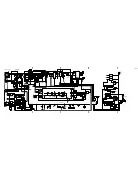
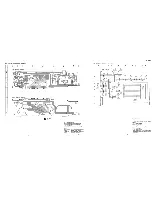
Page 10: ... 10 Connection Location CN501 CN701 MAIN Board Side A TP535 RFO TP534 VC TP524 TE ...
Page 12: ......
Page 13: ......
Page 14: ......
Page 15: ......


