


– 38 –
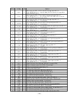
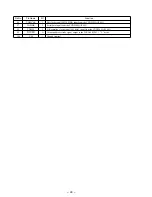
•
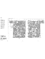
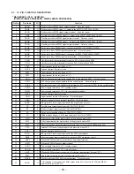
Pin No.
Pin Name
I/O
Function
1
SRON
O
Sled servo drive PWM signal output terminal Not used (open)
2
SRDR
O
Sled servo drive PWM signal (–) output to the MPC17A38ZVMEL (IC502)
3
SFON
O
Sled servo drive PWM signal output terminal Not used (open)
4
TFDR
O
Tracking servo drive PWM signal (+) output to the MPC17A38ZVMEL (IC502)
5
TRON
O
Tracking servo drive PWM signal output terminal Not used (open)
6
TRDR
O
Tracking servo drive PWM signal (–) output to the MPC17A38ZVMEL (IC502)
7
TFON
O
Tracking servo drive PWM signal output terminal Not used (open)
8
FFDR
O
Focus servo drive PWM signal (+) output to the MPC17A38ZVMEL (IC502)
9
FRON
O
Focus servo drive PWM signal output terminal Not used (open)
10
FRDR
O
Focus servo drive PWM signal (–) output to the MPC17A38ZVMEL (IC502)
11
FFON
O
Focus servo drive PWM signal output terminal Not used (open)
12
VCOO
O
Oscillator circuit output terminal for analog PLL of the playback EFM
13
VCOI
I
Oscillator circuit input terminal for analog PLL of the playback EFM
14
TEST
I
Input terminal for the test (fixed at “L”)
15
DVSS
—
Ground terminal (digital system)
16
TES2
I
Input terminal for the test (fixed at “L”)
17
TES3
I
Input terminal for the test (fixed at “L”)
18
PDO
O
Charge-pump output terminal for analog PLL of the playback EFM Not used (open)
19
VPCO
O
PLL charge-pump output terminal for the variable pitch Not used (open)
20
VCKI
I
Master clock signal (16.9344 MHz) input from the D/A converter (IC320) for the variable pitch
21
AVD2
—
Power supply terminal (+3.3V) (analog system)
22
IGEN
I
Power supply terminal (+3.3V) (for operational amplifier)
23
AVS2
—
Ground terminal (analog system)
24
ADII
I
Input terminal for the A/D converter Not used (open)
25
ADIO
O
Output terminal of the operational amplifier Not used (open)
26
RFDC
I
RF signal (DC level) input terminal for the digital servo process
27
TE
I
Tracking error signal input from the CXA1791N (IC501)
28
SE
I
Sled error signal input from the CXA1791N (IC501)
29
FE
I
Focus error signal input from the CXA1791N (IC501)
30
VC
I
Middle point voltage (+1.65V) input from the CXA1791N (IC501)
31
FILO
O
Filter output terminal for master clock of the playback master PLL
32
FILI
I
Filter input terminal for master clock of the playback master PLL
33
PCO
O
Phase comparison output terminal for master clock of the playback EFM master PLL
34
CLTV
I
Internal VCO control voltage input of the playback master PLL
35
AVS1
—
Ground terminal (analog system)
36
RFAC
I
RF signal (AC level) input terminal for the EFM demodulator
37
BIAS
I
Constant current input terminal of the playback EFM asymmetry circuit
38
ASYI
I
Playback EFM asymmetry comparator voltage input terminal
39
ASYO
O
Playback EFM full-swing output terminal
40
AVD1
—
Power supply terminal (+3.3V) (analog system)
41
DVDD
—
Power supply terminal (+3.3V) (digital system)
42
ASYE
I
Playback EFM asymmetry circuit on/off selection input terminal (fixed at “H”)
43
PSSL
I
Audio data output mode selection input terminal (fixed at “L”)
44
WDCK
O
Word clock signal (88.2 kHz) output terminal Not used (open)
45
LRCK
O
L/R sampling clock signal (44.1 kHz) output to the D/A converter (IC320) and MPEG
audio/video decoder (IC901)
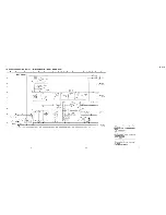
MAIN BOARD IC601 CXD2545Q
(DIGITAL SIGNAL PROCESSOR, DIGITAL SERVO PROCESSOR)
6-7.
IC PIN FUNCTION DESCRIPTION
Summary of Contents for D-V7000
Page 4: ... 4 SECTION 2 GENERAL This section is extracted from instruction manual ...
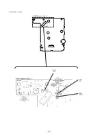
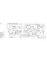
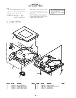
Page 10: ... 10 Connection Location CN501 CN701 MAIN Board Side A TP535 RFO TP534 VC TP524 TE ...
Page 12: ......
Page 13: ......
Page 14: ......
Page 15: ......


