TM150
ADJUSTMENTS, PERFORMANCE CHECK, AND FIRMWARE UPGRADE
2 – 38
CONFIDENTIAL
DRAFT
13 . THE DISPLAY DOES NOT APPEAR ON EXTERNAL DISPLAY (IN 65K COLOR MODE).
Does the display appear on Main Display?
Go to the section “Power is not turned on.”
Is External Display On/Off setting set to On?
Go to the setting as follows and set it to On:
Settings Phone
Settings External
Display Display On/Off
Is External Display unit fully inserted to CN703?
Improperly inserted to the connector.
Clean the contact point of the connector CN703 and insert the
unit again. Does the display appear?
The contact point of the connector is dirty.
Is 3 ± 0.1 V applied to CN703 pin 9?
Is R723 good in appearance and mounted properly?
R723 is defective or mounted improperly.
Are CN701 and CN103 good in appearance and mounted
properly?
CN703 and CN103 are defective or mounted improperly. And
FPC is defective.
Is 3.0 ± 0.1 V supplied from LCD_RST (CN703 pin 27 and
C751)?
IC707, C736, C751, and L749 are defective or mounted
improperly.
Is R222 good in appearance and mounted properly?
R222 is defective or mounted improperly.
Are C755, C756, and C758 good in appearance and mounted
properly?
Is electric potential normal at both ends of C755, C756, and
C757? Are rectangular waves sent?
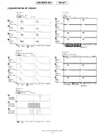
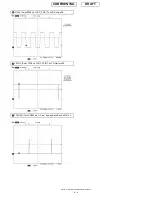
C755: rectangular wave of approx. 3 V
C756: rectangular wave of approx. 6 V
C757: rectangular wave of approx. 9 V
C755, C756, C757, and CN703 are defective, or External Dis-
play unit is defective.
Is approx. 11.8 V applied to CN703 pin 7 (TP717)?
Are the following voltages applied to V0 - V4?
V0 (C744): approx. 8.56 V
V1 (C745): approx. 7.33 V
V2 (C747): approx. 6.11 V
V3 (C748): approx. 2.42 V
V4 (C750): approx. 1.20 V
C744, C745, C747, C748, C750, CN703, and IC704 are
defective. The control signal line to IC704 or External Display
unit is defective.
* After a period of time the back light turns off, the voltage on TP717 decreases
to approx. 9 V.
External Display unit is defective.
NO
YES
NO
YES
NO
YES
YES
NO
NO
YES
NO
YES
NO
YES
NO
YES
NO
YES
NO
YES
Summary of Contents for TM150
Page 61: ...TM150 CIRCUIT DIAGRAM AND PWB LAYOUT 5 13 CONFIDENTIAL DRAFT MAIN PWB_FRONT ...
Page 62: ...TM150 CIRCUIT DIAGRAM AND PWB LAYOUT 5 14 CONFIDENTIAL DRAFT MAIN PWB_REAR ...
Page 63: ...TM150 CIRCUIT DIAGRAM AND PWB LAYOUT 5 15 CONFIDENTIAL DRAFT LCD PWB_FRONT ...
Page 64: ...TM150 CIRCUIT DIAGRAM AND PWB LAYOUT 5 16 CONFIDENTIAL DRAFT LCD PWB_REAR ...


