background image

TM150

CIRCUIT DIAGRAM AND PWB LAYOUT

5 – 2

CONFIDENTIAL

DRAFT

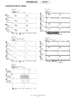
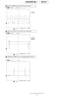
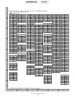
[3] WAVEFORMS OF CIRCUIT

RF Test Tool
Tx test
Data pattern ... TSC5

IP
(talking)
C811 
(IC801 23Pin)

IN
(talking)
C811 
(IC801 24Pin)

QP
(talking)
C812 
(IC801 25Pin)

QN
(talking)
C812 
(IC801 26Pin)

2

3

4

RF Test Tool
Rx test
channel_62, Gain 62dB, SniffOff

IP
(talking)
C811 
(IC801 23Pin)

IN
(talking)
C811 
(IC801 24Pin)

QP
(talking)
C812 
(IC801 25Pin)

QN
(talking)
C812 
(IC801 26Pin)

2

3

4

RF Test Tool
Rx test
GSM900 Band (channel 62)

SYNTHEN
(STAND-BY)
IC801 29Pin

SYNTHCLK
(STAND-BY)
IC801 30Pin

SYNTHDATA
(STAND-BY)
IC801 32Pin

6

5

7

BS1
(talking)
C870 
(IC803 10Pin)

BS2
(talking)
C871 
(IC803 6Pin)

BS3
(talking)
C872 
(IC803 12Pin)

BS4
(talking)
R1863 
(IC802 41Pin)

9

8

10

11

RF Test Tool
Tx test
GSM900 Band

Ch3

2.00 V

2.00 V

2.00 V

2.00 V

RF Test Tool
Tx test
DCS1800, PCS1900 Band

BS1
(talking)
C870 
(IC803 10Pin)

BS2
(talking)
C871 
(IC803 6Pin)

BS3
(talking)
C872 
(IC803 12Pin)

BS4
(talking)
R1863 
(IC802 41Pin)

9

8

10

11

Summary of Contents for TM150

Page 1: ...ecified should be used Caution Risk of explosion if battery is replaced by an incorrect type dispose of used batteries according to the instruction SERVICING CONCERNS CHAPTER 1 GENERAL DESCRIPTION 1 Specifications 1 1 2 Names of parts 1 2 3 Operation manual 1 3 CHAPTER 2 ADJUSTMENTS PERFORMANCE CHECK AND FIRMWARE UPGRADE 1 SHARP Program Support Tool SPST 2 1 2 Test points 2 48 3 Trouble shooting 2...

Page 2: ...erminals on the electric board microphone vibrator earpiece and speaker When handling these parts wear fingerstalls Should you touch these parts clean them with a soft dry cloth Always wear fingerstalls when handling a shield case on the electric board Otherwise oxidation may occur causing handset performance deterioration 7 The FPC is a precision device Handle it carefully to prevent any damages ...

Page 3: ...odel are subject to change without prior notice Powered by JBlendTM Copyright1997 2004 Aplix Corporation All rights reserved Java and all Java based trademarks and logos are trademarks or registered trademarks of Sun Micro systems Inc in the U S and other countries JBlend and all JBlend based trademarks and logos are trademarks or registered trademarks of Aplix Corporation in Japan and other count...

Page 4: ...DENTIAL DRAFT 2 NAMES OF PARTS No PARTS NAME 1 SPEAKER 2 SUB LCD 3 STRAP 4 CAMERA 5 CLOSE UP KNOB 6 PHONE JACK 7 SD CARD SLOT 8 BATTERY LOCK KNOB 9 EXT ANTENNA 10 SIDE KEY 11 I O CONNECTER 12 RECEIVER 13 MIC 1 8 12 13 2 5 9 10 11 4 3 6 7 ...

Page 5: ...1 3 CONFIDENTIAL DRAFT 3 OPERATION MANUAL Page numbers refer to the user guide OPTIONAL ACCESSORIES USB data cable The above accessories may not be available in all regions For details please contact your dealer QUICKSTART GUIDE ...

Page 6: ...TM150 GENERAL DESCRIPTION 1 4 CONFIDENTIAL DRAFT New Messages Download Games News Spor t 1 3 6 3 3 7 5 ...

Page 7: ...se Windows Explorer to execute the setup exe file on the CD ROM 2 The SPST TM150 setup wizard appears Follow the installation instructions 3 After the installation is complete shortcuts to SPST are created on the desktop and under the Start Programs TM150 menu Start SPST from the shortcuts 2 3 STARTING UP Connect TM150 to an operable serial port of the PC with the supplied data cable Make sure tha...

Page 8: ...to 4 5 RF calibration check RF Test Refer to 4 6 RF test tool User Password Reset Refer to 4 7 Password reset Performance check adjustment Refer to 4 8 Performance check and adjustment mode release Refer to 4 9 mode release Exit End SPST Parts Temperature adjustment Camera Temperature adjustment Battery Main display flicker adjustment White defect correction TH101 u F u u TH701 F u u u Main displa...

Page 9: ...ttings 4 Communication starts 5 The following appears when you select Yes in step 3 and MEPLOCK data exists Click Yes to restore the data 6 After the handset is turned on the initialization is complete 4 2 USER DATA BACK UP SPST saves all the data stored on the handset 1 Set the COM port on the SPST initial screen and click User Data Back up 2 Specify the file name in the following dialog box and ...

Page 10: ...describes how to install uninstall the software and how to connect handset to a PC 1 Installing uninstalling the software Connecting handset to a PC 1 Double click the setup exe icon in TM150 Install E folder 2 The Setup Wizard is activated Click the Next button 3 A location to install the software appears To install in the default location click the Next button To change the location click the Br...

Page 11: ...erating system While installing the upgrading tool in Windows 98 98 SE or ME a message may appear prompting to restart the operating system In this case restart your operating system follwoing the instruction Even if the message does not appear restart your operating system after the installation On Windows 98 if you start the upgrading tool without restarting the operation system the following me...

Page 12: ...a PC 2 Connect the cable to handset 3 The photo below shows handset connected to a PC B Using Communication Box 1 Connect a PC to Communication Box via a serial cable 2 Connect the AC charger to Communication Box and then plug it into the outlet All SET POWER SW on Communication Box must be turned off 3 Connect the conversion connector to Communication Box Cables Connect the conversion connector i...

Page 13: ...for upgrading When rewriting MOT files using the upgrading tool do not connect the AC charger to the cable If you connect the cable connected to the AC charger to handset charging starts and the MOT file rewrite operation is interrupted All SET POWER SW on Communication Box must be turned off If handset is connected with SET POWER SW turned on charging starts and the MOT file rewrite operation is ...

Page 14: ...eft appears alerting you a possible error Click the OK button to proceed and click the Cancel button to change the value You can shorten time for the MOT rewrite operation by selecting a smaller value for Wait Time Example Time to rewrite two MOT files at a time At the default setting 3 seconds rewrite time is approximately 40 minutes If the value is set to 1 the rewrite time will be reduced to ap...

Page 15: ...the hard disk first 4 Rewriting a MOT file Click the Start Loading Flash button to start rewriting 1 Press Power Button appears When using a cable for upgrading Hold down the Power key When using the Communication Box Turn on Communication Box SW from No 10 down to No 1 turn on only the handsets you are using 2 Keep Pressing Power Button appears When using a cable for upgrading Hold down the Power...

Page 16: ... the default Wait Time 3 seconds increase the value Consequently this will increase the time to complete the rewrite operation 5 Checking the value of SUM When the rewrite operation is completed a confirmation message appears with SUM SUM also appears on handset When using a cable for upgrading After 8 seconds SUM disappears When using Communication Box When SET POWER SW is turned off SUM disappea...

Page 17: ...ons Select a COM port connected to the PC cable 6 RAM Loader not responding to Commands No response from Loading loader Start over the rewrite operation 7 RAM Loader responding Parameter Error Information sent from the PC is illegal Reinstall the upgrading tool Start over the rewrite operation 8 RAM Loader responding Flash Error XXXX Failed to initialize FLASH ROM in XXXX Start over the rewrite op...

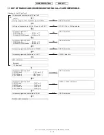
Page 18: ... The initial screen returns 4 5 4 RF performance check Insert SIM card 1 Apply 4 V using a stabilized power supply and turn on the handset 2 Start RF calibration check on SPST and click Calibration 3 When initialization is complete click OK 4 Apply 4 V using a stabilized power supply and turn on the handset After the handset enters Standby mode lower the voltage to 3 7 V 5 Make sure the handset is...

Page 19: ...ck starts 8 The following message appears during the check Press the keys 1 2 3 and Send again and click OK 9 Make sure the terminal display is In Call and click OK 10 RF performance check is complete Click Save As and name the file to save the result Click OK to exit The following will be displayed in case of failure See the attachment 2 for troubleshooting 11 Click OK 12 The initial screen retur...

Page 20: ... PCL5 44 Mod_spectrum 800 124CH PCL5 45 Mod_spectrum 800 37CH PCL11 46 Mod_spectrum 600 37CH PCL11 47 Mod_spectrum 400 37CH PCL11 GSM900 Tx 48 Mod_spectrum 250 37CH PCL11 49 Mod_spectrum 200 37CH PCL11 50 Mod_spectrum 200 37CH PCL11 51 Mod_spectrum 250 37CH PCL11 52 Mod_spectrum 400 37CH PCL11 53 Mod_spectrum 600 37CH PCL11 54 Mod_spectrum 800 37CH PCL11 55 Mod_spectrum 800 37CH PCL19 56 Mod_spect...

Page 21: ... 699CH PCL0 139 Mod_spectrum 800 512CH PCL0 Band Sending Receive No Item to be inspected Channel PCL DCS Tx 140 Mod_spectrum 600 512CH PCL0 141 Mod_spectrum 400 512CH PCL0 142 Mod_spectrum 250 512CH PCL0 143 Mod_spectrum 200 512CH PCL0 144 Mod_spectrum 200 512CH PCL0 145 Mod_spectrum 250 512CH PCL0 146 Mod_spectrum 400 512CH PCL0 147 Mod_spectrum 600 512CH PCL0 148 Mod_spectrum 800 512CH PCL0 149 ...

Page 22: ...CL0 230 Burst Power 512CH PCL0 231 Burst Power 810CH PCL0 Band Sending Receive No Item to be inspected Channel PCL PCS Tx 232 Burst Power 661CH PCL5 233 Burst Power 661CH PCL15 234 Frequency Error 661CH PCL0 235 Frequency Error 512CH PCL0 236 Frequency Error 810CH PCL0 237 Phase Error RMS 661CH PCL0 238 Phase Error RMS 512CH PCL0 239 Phase Error RMS 810CH PCL0 240 Phase Error Peak 661CH PCL0 241 P...

Page 23: ... 810CH PCL0 315 Switch_Spectrum 1200 810CH PCL0 316 Switch_Spectrum 1800 810CH PCL0 317 Switch_Spectrum 1800 661CH PCL5 318 Switch_Spectrum 1200 661CH PCL5 319 Switch_Spectrum 600 661CH PCL5 320 Switch_Spectrum 400 661CH PCL5 321 Switch_Spectrum 400 661CH PCL5 322 Switch_Spectrum 600 661CH PCL5 323 Switch_Spectrum 1200 661CH PCL5 324 Switch_Spectrum 1800 661CH PCL5 Band Sending Receive No Item to ...

Page 24: ...OM port to which Data Cable is connected 5 Press the Initialize Read Data button 6 The figre shown below appears wait a few seconds 7 Click OK to proceed 4 6 3 Tests 1 BAND Select Channel Select a band and a channel to test Settings are applied to all tests Procedure 1 Select a band GSM900 DCS or PCS 2 Select or enter a channel using Channel bar or Input box Hook Hook Hook PWB Hook Hook Hook Red P...

Page 25: ...he handset receives burst signals in this test PCL bar TX frequency of selected channels Current PCL Read only TX ON OFF button This indicator appears during burst transmission Data patterns PCL GSM900 Tolerance dBm 5 33 2 dB 6 31 3 dB 7 29 3 dB 8 27 3 dB 9 25 3 dB 10 23 3 dB 11 21 3 dB 12 19 3 dB 13 17 3 dB 14 15 3 dB 15 13 3 dB 16 11 5 dB 17 9 5 dB 18 7 5 dB 19 5 5 dB PCL DCS PCS Tolerance dBm 0...

Page 26: ...1 Continuous sine wave without modulation with the frequency as follows Frequency of the measured channel 67 708kHz Ex channel GSM 37ch 3 the result 942 467708 MHz Power 110 to 10 dBm 2 BCCH signal of the measured channel Power 110 to 10 dBm Result When the handset is properly calibrated the error between Esti mated Power and Measured Power is less than 3dB 4 6 4 Termination Turn off the handset t...

Page 27: ...ot recognized in 3 Troubleshooting 4 8 7 Vibrator test Click to vibrate the handset Click OK to exit If a failure occurs see 5 Vibrator does not work in 3 Trouble shooting 4 8 8 Melody test A message describes test items Click Yes to proceed and No to exit The order of the test items speaker 3 hands free 3 hands free stereo 3 speaker analog melody 4 8 9 Audio test The following appears Select a te...

Page 28: ...e of 20 cm from a fluorescent light and adjust the value to minimize flicker on the display with the b and c buttons Click Save and confirm that the main display does not flicker Fine adjustment for DC voltage between display electrodes 4 8 15 External display contrast adjustment Click the External display contrast adjustment button The following screen appears Trouble found by SPST 1 Handset micr...

Page 29: ...ht sensor appear as black points in the dis play even when a captured image is completely white display is all white Perform black defect correction to eliminate errors in these pixels 1 Requirements Desk top type of fluorescent lamp Black defect correction sheet Illuminance meter 2 Procedure 1 Cover the camera section with the black defect correction sheet as shown in Figure 96 2 Check the distan...

Page 30: ...Retry To exit click Cancel 3 When complete the following message appears 5 OTHER TESTS SPST does not provide tests of Bluetooth USB communication Check them according to the following instructions 5 1 USB Connect TM150 and a PC with a USB cable Check that TM150 is recognized as a device If the USB driver for TM150 SHARP GSM GPRS USB Driver is not installed on the PC Found New Hardware window appea...

Page 31: ...TP183 Flexible PWB insert check terminal 3 TP124 PWRON TP184 Flexible PWB insert check terminal 4 TP126 SP1 TP502 VBAT TP127 SP2 TP503 VBAT TP144 Terminal for STACK MEMORY adhesion check 1 TP506 BATT_SENSE TP147 Terminal for STACK MEMORY adhesion check 2 TP514 BT_VCC 3 0V TP153 VPP Flash TP515 VBUS_IN TP157 Analog Power Supply IC INT TP521 POWONKEY TP158 VINT 3V TP523 USB D TP160 HEDSET_DET TP524 ...

Page 32: ...S PERFORMANCE CHECK AND FIRMWARE UPGRADE 2 26 CONFIDENTIAL DRAFT TP No Signal name TP No Signal name TP111 VVIB TP505 DGND TP112 DGND TP520 BATT TP501 BATT TP522 POWONKEY TP504 DGND TP534 BATT_SENSE MAINPWB B REARSIDE ...

Page 33: ...Terminal for APPLICATION POWER adhesion check 2 TP728 LEDCTL TP709 VDD6 3 1V TP729 LEDR TP710 Backlight LED TP730 LEDG TP711 Backlight LED TP731 LEDB TP712 CAMCLK TP732 Power supply for camera 15V TP713 13MHzCLK TP733 Power supply for camera 8V TP714 VLCD 1 8V TP734 RECIVER_OUTN TP715 Terminal for LCDC adhesion check 1 TP735 RECIVER_OUTP TP716 Terminal for LCDC adhesion check 2 TP736 AVDD 3 1V TP7...

Page 34: ...TM150 ADJUSTMENTS PERFORMANCE CHECK AND FIRMWARE UPGRADE 2 28 CONFIDENTIAL DRAFT TP No Signal name TP No Signal name TP703 SP1 TP704 SP2 LCD PWB REAR SIDE ...

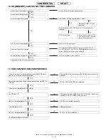
Page 35: ...ack memory IC101 and IC106 are defective Program code of 5 level stack memory IC101 is garbled YES NO YES NO NO YES YES NO NO YES Connect a battery of 4 0 V or more Is 3 6 V or more applied to BATT terminal TP520 Battery terminals are defective connector terminal is dirty or soldering is improper Is the voltage 1 2 V or lower on SENSE terminal TP506 The battery is defective or set improperly Is th...

Page 36: ...NO YES YES NO NO YES NO YES NO YES NO YES NO YES YES NO Hands free kit headset The following procedure applies to both monaural and stereo headsets Replace the hands free kit Is the signal sent Hands free kit is defective R104A R112 and V101 are defective Is 0 7 1 8 V applied to JK101 pin 2 Is 0 7 1 8 V applied to TP120 Is 2 4 2 5 V applied to TP176 R122 is defective Is 2 4 2 5 V applied to IC103 ...

Page 37: ... pin 60 R124 is defective Is the voltage 0 V on R192 IC106 pin 89 side Jack JK101 is defective or the jack plug is in a poor contact with hands free kit Handset mode is set Is approx 1 2 V applied to IC103 pin 60 IC103 is defective IC103 or IC106 is defective YES NO YES NO YES NO NO YES NO YES YES NO YES NO YES NO YES NO YES NO NO YES NO YES Hands free kit stereo headset Option The headset cannot ...

Page 38: ... L at R701 Set a battery of 4 0 4 2 V Click the Performance check adjustment button on SPST LED702 of the mobile light is defective For settings and connections for SPST refer to the ADJUSTMENTS PERFORMANCE CHECK AND FIRMWARE UPGRADE see page 2 1 Click the Temperature adjustment button Is the value of temp normal Measurement tolerance 5 deg TH701 TH101 and IC103 are defective CN701 and CN103 are c...

Page 39: ... back up battery holder properly installed to SD SIM FPC The remaining power of back up battery is insufficient Back up battery is defective Back up battery holder is defective SD SIM FPC is broken or CN104 is defective R254 is defective Is 1 5 V or more applied to TP167 without a battery in the handset IC103 is defective X101 R169 R174A and C176 are defective NO NO YES YES NO YES When ring tones ...

Page 40: ...is defective Go to Hands free kit monaural headset in the section No voice is heard from the earpiece YES YES NO NO NO YES YES NO YES NO NO YES YES NO NO YES YES NO Speaker Are keypad tones and ring tones normal Go to the section Speaker does not work In Playback window does playback start normally and the capacity bar change IC101 or IC106 is defective Not defective Is Ringer Volume set to Silent...

Page 41: ...k light FPC or CN705 is defective Is the contact point of back light FPC clean Is back light FPC properly inserted to CN705 Clean back light FPC and insert it again Does it turn on Not defective Is 13 24 V applied between TP710 and TP711 Back light FPC is defective Are C790 C791 C702 C707 C713 R718 and D702 in good appearance and mounted properly C790 C791 C702 C707 C713 R718 and D702 are defec ti...

Page 42: ...SM900 bands IC803 pin 15 DCS1800 PCS1900 bands IC803 pin 13 IC802 is defective Is frequency signal supplied to pin 1 of FL905 IC803 is defective Is frequency signal supplied to pin 1 of J801 FL905 is defective J801 is defective Receiver 70 dBm input Is frequency signal supplied GSM900 bands IC801 pins 9 10 DCS1800 band IC801 pins 6 7 PCS1900 band IC801 pins 3 4 IC801 is defective Is frequency sign...

Page 43: ... to the section Power is not turned on Is 3 0 0 1 V supplied from LCD_RST L746 Are L746 C736 C751 CN701 and CN703 good in appear ance and mounted properly L746 C736 C751 CN701 and CN703 are defective or mounted improperly Is 3 0 V 0 1 V applied to CN704 pins 34 37 and 38 Are R737 R738 C774 and C775 good in appearance and mounted properly CN404 R737 R738 C774 and C775 are defective or mounted impro...

Page 44: ... 0 0 1 V supplied from LCD_RST CN703 pin 27 and C751 IC707 C736 C751 and L749 are defective or mounted improperly Is R222 good in appearance and mounted properly R222 is defective or mounted improperly Are C755 C756 and C758 good in appearance and mounted properly Is electric potential normal at both ends of C755 C756 and C757 Are rectangular waves sent C755 rectangular wave of approx 3 V C756 rec...

Page 45: ...04 is defective Is 3 1 V applied to TP709 Is 3 0 V applied to IC702 pin 1 Regulator IC702 is defective Is 3 1 V applied to pin 35 of camera module CN701 is defective Camera relay FPC is broken IC707 or peripheral circuits are defective Is 15 V applied to TP732 Does the LED of the flash work properly IC707 or peripheral circuits are defective Also IC704 or the control line is defective CN701 is def...

Page 46: ... after the power is turned on Is 2 85 V supplied from pins 1 2 and 6 of the SIM card And is periodic pulse wave 3 25 MHz sent from pin 3 of the SIM card The contact point of the SIM card connector is deformed or dirty Replace C210 or C159 Is 2 85 V supplied from CN104 pin 28 Are C210 and C159 good in appearance and mounted prop erly IC103 is defective Replace R195 or C216 Is 2 85 V supplied from C...

Page 47: ...WB are broken or short cir cuited IC106 is defective or has come off After formatting can the SD card be used IC106 is defective or has come off File system on the SD card is damaged NO YES YES NO YES YES NO YES NO NO YES NO YES NO YES Connect a properly working handset to the Data USB cable that is not recognized Is it recognized Reinstall the driver and replace the USB cable to connect the hands...

Page 48: ...rame L and R and remove the closeup lever When installing squeeze the camera closeup lever 3 Remove the speaker from the cabinet B unit C VIBRATING MOTOR REMOVAL 1 Open the display section Remove the screw cover and remove the special screw When removing or installing the special screw use the exclusive tool When tightening the screws follow the tightening sequence of a b c and d 2 Disengage the p...

Page 49: ...ence line b and the SIM connector end face reference line c as the reference Attach the ANT dust prevention sheet d so that it is fit with the RF external antenna connector with the PWB silk section as the reference Attach the submersion sheet e inside the bump area When attaching the PWB unit rotate the main PWB and the LCD PWB 180 degrees in the arrow direction to wind the flat cable 2 Remove th...

Page 50: ...m the main LCD holder unit Remove the BL flexible unit Hold the both ends of the main LCD as shown in the figure and never press TAB a H RECEIVER AND MIC REMOVAL 1 Remove the receiver and the mic from the cabinet A C unit When attaching the mic use care to set so that the spring direction is vertical to the cabinet a ...

Page 51: ...UT1 2 Speaker Accessary Connector VCHG Li ION Battery 720mAh ADR280 REFEN REF VSIM Back up Battery RECEIVER AOUT1P Headset Jack AOUT3R AIN1P AIN1N MIC AIN2P AIN2N AOUT3L ADDRESS DATA BUS GPIO INT ADDRESS DATA BUS GPIO INT AD6535 Typhoon Filter Filter Voltage Reference BUFFER POWER ON RESET GENERATOR AFC DAC Ramp RAM RAMP DAC Filter AUX ADC Analog SW DAC Filter PGA DAC Tone Generator PGA ADC Filter...

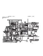
Page 52: ...Loop filter 90deg Shift PGA Test Connector VBAT 900 1800 1900 90 deg Shift 1 2 SAW Filter 4 PCS RX DCS RX SYNTHEN D SYNTHDATA D SYNTHCLK D 1 2 Serial data interface VRF TCXOEN D VBAT LNA LNA LNA GSM900 RX BS 2 BS4 VTCXO RX Line Control Line TX Line BS1 BS2 BS3 DPD Voltage Regulator D Digilal A Analog PA APC SAW Filter IC802 RF3146 IC803 FL902 J801 IC801 HD155155 IC804 TCX801 FL903 1800 1900 900 1 ...

Page 53: ...hassis with no signal given Conditions SIM card inserted power on in stand by mode opened Schematic diagram and Wiring Side of P W Board for this model are subject to change for improvement without prior notice Parts marked with are important for maintaining the safety of the set Be sure to replace these parts with specified ones for main taining the safety and performance of the set 2 TYPES OF TR...

Page 54: ...king C812 IC801 25Pin QN talking C812 IC801 26Pin 2 3 4 RF Test Tool Rx test GSM900 Band channel 62 SYNTHEN STAND BY IC801 29Pin SYNTHCLK STAND BY IC801 30Pin SYNTHDATA STAND BY IC801 32Pin 6 5 7 BS1 talking C870 IC803 10Pin BS2 talking C871 IC803 6Pin BS3 talking C872 IC803 12Pin BS4 talking R1863 IC802 41Pin 9 8 10 11 RF Test Tool Tx test GSM900 Band Ch3 2 00 V 2 00 V 2 00 V 2 00 V RF Test Tool ...

Page 55: ...C803 12Pin BS4 talking C874 IC803 14Pin 9 8 10 11 RF Test Tool Rx test PCS1900 Band BS1 talking C870 IC803 10Pin BS2 talking C871 IC803 6Pin BS3 talking C872 IC803 12Pin BS4 talking C874 IC803 14Pin 9 8 10 11 13MHz IN Point R261 To Digital Base Band LSI Pin142 13MHz OUT Point R166 from Digital Base Band LSI Pin84 32 768KHz IN Point R152 To Digtal Base Band LSI Pin49 12 13 14 ...

Page 56: ...RCUIT DIAGRAM AND PWB LAYOUT 5 4 CONFIDENTIAL DRAFT DCLK Point R759 on LCDC_PCB To LCD Unit pin26 VSYNC Point C760 on LCDC_PCB To LCD Unit pin28 TCXOEN Point IC804 pin 1 From Analog Base Band LSI Pin 2 15 16 17 ...

Page 57: ...CONFIDENTIAL DRAFT CONFIDENTIAL DRAFT TM100 CIRCUIT DIAGRAM AND PWB LAYOUT 5 5 TM100 CIRCUIT DIAGRAM AND PWB LAYOUT 5 6 8 7 6 5 4 3 2 1 A B C D 1 2 3 4 5 6 7 8 D C B A BASE BAND MAIN ...

Page 58: ...CONFIDENTIAL DRAFT CONFIDENTIAL DRAFT 8 7 6 5 4 3 2 1 A B C D 1 2 3 4 5 6 7 8 D C B A RF PORT MAIN TM100 CIRCUIT DIAGRAM AND PWB LAYOUT 5 7 TM100 CIRCUIT DIAGRAM AND PWB LAYOUT 5 8 ...

Page 59: ...CONFIDENTIAL DRAFT CONFIDENTIAL DRAFT KEY MAIN 8 7 6 5 4 3 2 1 A B C D 1 2 3 4 5 6 7 8 D C B A TM100 CIRCUIT DIAGRAM AND PWB LAYOUT 5 9 TM100 CIRCUIT DIAGRAM AND PWB LAYOUT 5 10 ...

Page 60: ...CONFIDENTIAL DRAFT CONFIDENTIAL DRAFT TM100 CIRCUIT DIAGRAM AND PWB LAYOUT 5 11 TM100 CIRCUIT DIAGRAM AND PWB LAYOUT 5 12 8 7 6 5 4 3 2 1 A B C D 1 2 3 4 5 6 7 8 D C B A LCD ...

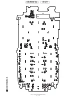
Page 61: ...TM150 CIRCUIT DIAGRAM AND PWB LAYOUT 5 13 CONFIDENTIAL DRAFT MAIN PWB_FRONT ...

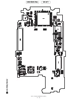
Page 62: ...TM150 CIRCUIT DIAGRAM AND PWB LAYOUT 5 14 CONFIDENTIAL DRAFT MAIN PWB_REAR ...

Page 63: ...TM150 CIRCUIT DIAGRAM AND PWB LAYOUT 5 15 CONFIDENTIAL DRAFT LCD PWB_FRONT ...

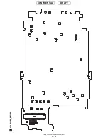
Page 64: ...TM150 CIRCUIT DIAGRAM AND PWB LAYOUT 5 16 CONFIDENTIAL DRAFT LCD PWB_REAR ...

Page 65: ... E CN704 TO MAIN PWB A REAR SIDE 5 14 8 D CN705 TO MAIN PWB A REAR SIDE 5 14 8 B CN701 MAIN PWB A FRONT SIDE 5 13 3 G TO MAIN PWB A REAR SIDE 5 14 12 G TO MAIN PWB A REAR SIDE 5 14 9 G SOLDER SOLDER BACK LIGHT FPC PWB C B TO MAIN PWB A REAR SIDE 5 14 12 G E A TO KEY PWB B REAR SIDE 5 28 11 A C TO KEY PWB B FRONT SIDE 5 27 4 A D CN102 TO KEY PWB B REAR SIDE 5 28 9 A CN104 TO KEY PWB B REAR SIDE 5 2...

Page 66: ...V Not used 0V 0 01V 0V 0V 0V IC107 PIN NO VOLTAGE 1 2 3 2 98V 0V 2 98V IC108 PIN NO VOLTAGE 1 2 3 4 IC111 PIN NO VOLTAGE 1 2 3 4 5 IC113 PIN NO VOLTAGE 1 2 3 4 5 0V 2 98V 0V 0V 2 98V IC109 PIN NO VOLTAGE 1 2 3 4 5 0V 0V 0V 0V 3 69V IC114 PIN NO VOLTAGE 1 2 3 4 5 IC115 PIN NO VOLTAGE 1 2 3 4 0V 0V Not used 0V IC116 PIN NO VOLTAGE 1 2 3 4 0V 0 14V 0V 0 14V IC508 PIN NO VOLTAGE 1 2 3 4 0V 3 69V 2 99V...

Page 67: ...te High Z High impedance 27 A21 Input Address input NOR Flash Smartcombo RAM 2 28 SC2 CE2 Input Sleep state input Smartcombo RAM 2 29 DQ13 Input Output Data input output NOR Flash Smartcombo RAM SRAM Command Address and Data input output Smartcombo Flash 30 DQ6 Input Output Data input output NOR Flash Smartcombo RAM SRAM Command Address and Data input output Smartcombo Flash 31 DQ4 Input Output Da...

Page 68: ...ess input NOR Flash Smartcombo RAM SRAM 72 A1 Input Address input NOR Flash Smartcombo RAM SRAM 73 SC1 CE1 Input Chip enable input Smartcombo RAM 1 74 NC Not used 75 NC Not used 76 NC Not used Pin No Terminal name Input Output Description of terminal 77 SF WP Input Write protect input Smartcombo Flash 78 SF CE Input Chip enable input Smartcombo Flash 79 A5 Input Address input NOR Flash Smartcombo ...

Page 69: ...ion supply 2 75 3 3 V 49 BSOFS Output Baseband serial port output framing signal 50 BSDI Input Baseband serial port data input 51 VBAT2 Input Analog baseband regulator input 52 NC_G16 Not used 53 CSDO Output Control serial port data output 54 CSDI Input Control serial port data input 55 VBAT2 Input Analog baseband regulator input 56 VABB Output Analog baseband supply 57 ASM Input Advanced state ma...

Page 70: ...nd for power supply 143 AGND0 Thermal ground for power supply 144 AGND0 Thermal ground for power supply 145 AGND0 Thermal ground for power supply 146 AGND0 Thermal ground for power supply 147 AGND0 Thermal ground for power supply 148 AGND0 Thermal ground for power supply Pin No Terminal name Input Output Description of terminal Pin No Terminal name Input Output Description of terminal 1 CLKI Input...

Page 71: ... supply 1 7 1 9 V VCORE 32 KEYPADCOL 3 Output KEYIN signal output 3 33 KEYPADCOL 2 Output KEYIN signal output 2 34 GPIO_39 Output USB PU control for interface IC 35 GPIO_37 Input Interrupt input from analog BB 36 GPIO_34 Output UART_TXD for Bluetooth module 37 ADD 4 Output Processor address bus 4 38 ADD 2 Output Processor address bus 2 39 GND Ground 40 KEYPADROW 0 Input KEYIN signal input 0 41 VEX...

Page 72: ...dress bus 23 109 GND Ground 110 VEXT Input SIM power supply 2 4 3 3 V VINT 111 GND Ground 112 GPIO_4 Output UART_CTS for Bluetooth module 113 GPIO_2 Output USB charge current control 114 GPIO_3 Input UART_RTS for Bluetooth module Pin No Terminal name Input Output Description of terminal 115 DATA 2 Input Output Processor data bus 2 116 DATA 0 Input Output Processor data bus 0 117 DATA 5 Input Outpu...

Page 73: ...GPO_4 Output Mode select 1 for interface IC 182 GPO_7 Output Bluetooth module power ON OFF control 183 GPO_16 Output Band select 1 for RF BS1 184 GPO_17 Output Band select 2 for RF BS2 185 NHWR NUSB Output Processor high write strobe 186 GPO_19 Output Mode select 3 for interface IC 187 NLWR NLSB Output Processor low write strobe 188 NWAIT Input Processor wait input 189 NRESET Input System reset in...

Page 74: ... ECO Input High speed low consumption selector switch 5 VOUT Output Output Pin No Terminal name Input Output Description of terminal 1 A Input Signal input 2 B Input Signal input 3 GND Ground 4 Y Output Logic value output 5 VCC Input Power supply 5 1 2 VOUT NB 4 3 Bandgap Reference Thermal Protection VIN CONT GND 5 4 2 VDD CE GND VOUT ECO VREF CURRENT LIMIT 3 1 1 A B GND VCC TOP VIEW Y 2 3 5 4 Pin...

Page 75: ... NC TXANAIN RXANAOUT USBD RXD CPU_USB_D CPU_USB_D REG33 PU15 PUEA GND3 RXANAIN TXANAOUT MODESEL3 BCNT BDATA UART_CTS 19 15 16 17 MODE 0 1 2 ON MODE 3 5 OFF CPUVDD CPUVDD CPUVDD CPUVDD DEC H ON L OFF CPUVDD CPUVDD CPUVDD CPUVDD CPUVDD CPUVDD MODE 0 1 2 OFF MODE 3 5 ON MODE 0 2 3 OFF MODE 1 5 ON MODE 0 2 3 5 OFF MODE 1 ON MODE 0 2 3 5 L MODE 1 H MODE 0 2 3 5 L MODE 1 H MODE 0 2 3 5 L MODE 1 H MODE 0...

Page 76: ...put Output For factory use only Not used 33 PIO2 Input Output General purpose I O 34 PIO0 Input Output General purpose I O Pin No Terminal name Input Output Description of terminal 1 INB Input Input B 2 INA Input Input A 3 GND Ground 4 OUT Y Output Output Y 5 VCC Power supply 1 IN B IN A GND TOP VIEW VCC OUT Y 2 3 5 4 Pin No Terminal name Input Output Description of terminal 1 VSS Ground GND 2 VIN...

Page 77: ...nal Display is active when CS_B is Low 23 VDDIO IO Power supply 3 0 V 2 7 V 3 3 V 24 LCDINT Output External interrupt signal Starting varies when interruption occurs 25 GTDIO_B Output MPEG4ASIC internal core power cut signal Low is active 26 VDDIO IO Power supply 3 0 V 2 7 V 3 3 V 27 SUBDB1 Input Output Data bus for External display 28 BDATA 5 B5 Output Display panel B output signa 29 BDATA 5 B4 O...

Page 78: ...gic ground Pin No Terminal name Input Output Description of terminal 84 VDDCORE CORE Power supply 1 8 V 1 6 V 2 0 V 85 CAMCK Output Clock for camera operation 86 GDATA 1 G1 Output Display panel G output signal 87 GDATA 0 G0 Output Display panel G output signal 88 RDATA 5 R5 Output Display panel R output signal 89 RDATA 4 R4 Output Display panel R output signal 90 VDDCORE CORE Power supply 1 8 V 1 ...

Page 79: ...ad signal 2 for 4 wire serial IF General purpose PORT output default 131 BUFOFF_B Input Buffer Gated switching signal for I O through current prevention High when Host_IF signal is activated 132 VDDIO IO Power supply 3 0 V 2 7 V 3 3 V 133 DUMMY2 Dummy 2 134 SE_LD3 PORT6 Output Load signal 3 for 4 wire serial IF General purpose PORT output default Not used 135 VDDIO IO Power supply 3 0 V 2 7 V 3 3 ...

Page 80: ...hExpand RED Pallet BLUE Pallet CDE DCS_B DA 1 0 EXCS_B 3 0 ADDRESS DECODE SE_DI PORT7 Memory Interface 72bit BS_DATA 71 0 SEL Buffer 18bitx4 Buffer 18bitx4 Some MHz to 68 MHz PLL Dividing Oscillation circuit Current consumption is decreased in a standby mode Some MHz to 33 MHz Approx 16 128 MHz External MPEG4_ASIC External CAMERA_DSP 4 wire SO PO 6 bit x 4 Available for magnification function CPU ...

Page 81: ...3 2 4 times step up charge pump C2 connection terminal Step up stop 20 VIO GND2 Logic system power supply terminal 21 VPLUS2 Input GND1 DC DC step up voltage feedback input for R G B LED Step up stop 22 CAPN2 Output CPIN GND3 2 4 times step up charge pump C2 connection terminal Not used Step up stop 23 GND3 VBAT1 Ground 24 STRB I CMOS input VIO VIO GND2 Three wire serial strobe input 25 CLK I CMOS...

Page 82: ...for TXVCO 15 GNDTXVCOD GND for DCS PCS TxVCO 16 GNDTXVCODB GND for DCS PCS TxVCO 17 TXOUTG Output Tx output for GSM 18 COMMONGND GND for common 19 TXOUTD Output Tx output for DCS PCS 20 TXVCOGB Input Negative TxVCO output for GSM 21 TXVCOG Input Positive TxVCO output for GSM 22 VCCIQ Input VCC for IQ modulator 23 IOUT IIN Input Output Positive output input of I channel modulator 24 IOUTB IINB Inpu...

Page 83: ...rnal circuit node Do not externally connect 28 NC Internal circuit node Do not externally connect 29 NC Internal circuit node Do not externally connect 30 GND Internally connected to the package base 31 DCS PCS OUT RF output for the DCS PCS bands This is a 50Ω output The output matching circuit and DC block are internal to the package 32 GND Internally connected to the package base 33 NC Internal ...

Page 84: ... select input 40 WRB Input IP parameter write signal 41 CINT Output Interruption signal 42 VDD3 Power supply input 15 V Sensor 1 42 Pin No Terminal name Input Output Description of terminal 1 T COM Input COM electric potential input for CS 2 T COM Input COM electric potential input for CS 3 TFT COM Input COM voltage input 4 COMC Output COM signal output 5 COMC Output COM signal output 6 COMDC Outp...

Page 85: ...ut Register select signal 0 Display RAM data 1 Command data 10 WRB Input Write signal L Activated 11 RDB Input Read signal L Activated Pin No Terminal name Input Output Description of terminal MAIN DISPLAY 59 1 To InputTerminal 12 D0 Input Output Data signal 13 D1 Input Output Data signal 14 D2 Input Output Data signal 15 D3 Input Output Data signal 16 D4 Input Output Data signal 17 D5 Input Outpu...

Page 86: ...Japan 2004 June Printed in Japan t COPYRIGHT 2004 BY SHARP CORPORATION All rights reserved Printed in Japan No part of this publication may be reproduced stored in a retrieval system or transmitted In any form or by any means electronic mechanical photocopying recording or otherwise without prior written permission of the publisher ...

Reviews: