background image

10

2.2.Computer analog signal input circuit
IBM computer and APPLE computer output the following analog signals at the load of 75

.

The signals are converted into 8-bit digital signals by the A/D converter(IC315~317).
The computer analog signals are given to Pin 21 of the A/D converter, are divided by 256
between the voltages given to Pin 18(VRT) and Pin 24(VRB), and are digitally converted.
The following table shows the reference voltage which is given to the A/D converter.

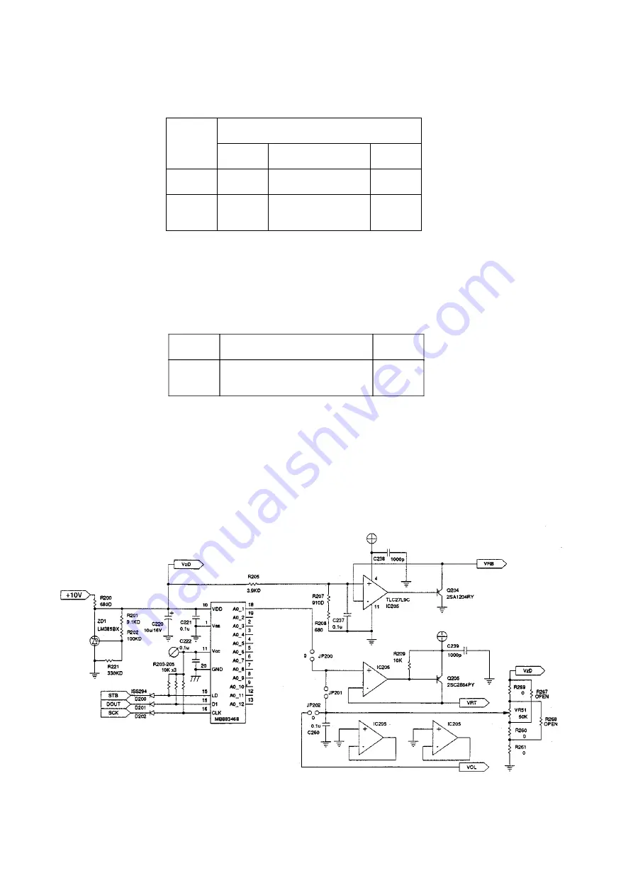
2.3.Threshold level generation circuit
In order to convert the computer and composite analog signal into digital, it is necessary to set
the threshold level on the A/D converter.  As shown in Fig. 3, VRT and VRB voltages are set
on the basis of the reference power of ZD1.  VRT can be varied by key operation.
As the adjusting method from the main body, the MENU button and SELECT button are used
to display the contrast adjustment in the screen and to allow the set value to be changed with
UP and DOWN selector buttons.

Fig. 3 Threshold Level Generation Circuit

Table 2

Computer Analog Signal

R

G

B

IBM

0.7Vp-p

0.7Vp-p

0.7Vp-p

APPLE

0.7Vp-p

1.0Vp-p

(Synchronization signal 

overlapped)

0.7Vp-p

Table 3

VRT

VRB

Threshold 
Level

3.8V(2.8~4.8V)

Adjustment are possible

1.0V

Summary of Contents for QD-101MM

Page 1: ...IRCUIT DESCRIPTION 8 5 TROUBLESHOOTING CHART 21 6 CIRCUIT DIAGRAM PWB 38 7 REPLACEMENT PARTS LIST 54 8 ASSEMBLY DRAWINGS 60 9 INFORMATION 64 QD 101MM In the interests of user safety the set should be restored to it s original condition and only parts identical to those specified be used TFT DISPLAY UNIT MODEL QD 101MM ...

Page 2: ...on an external control terminal has been provided to facilitate control of the display unit s functions The power source is an external AC adaptor that provides 12V DC to display monitor unit This unit can be used with the following models and signals 1 Personal computers 1 IBM PC XT PC AT PS 2 PS 1 PS 55 Think Pad 700 2 Apple MACII MAC SE MACIIcx MACIIci MACIIsi MAC LC Power Book 160 180 Quadra 3...

Page 3: ...1 Composite video input connector 1 S terminal video signal input connector 1 Audio input connector 1 12V DC input socket 1 7 Switches and others Power switch MENU button 1 SELECT button 1 UP button 1 DOWN button 1 RESET button 1 8 Adjustment Color adjustment Brightness adjustment Tint adjustment Contrast adjustment Audio level adjustment Image horizontal vertical position adjustment Phase adjustm...

Page 4: ...nput section Input pin HEC0470 01 640 Hoshiden Co Ltd or equivalent Center pin AC adaptor Accessory AC adaptor DADP 2004PAZZ Input voltage DC12V when main body is loaded 2 5 S terminal video signal input section Signal layout 1 GND 2 GND 3 Y signal 4 C signal Pin No Analog Signal Digital Signal 1 Analog Red N C 2 Analog Green Digital Green 3 Analog Blue Digital Blue 4 N C Digital Secondary Red r 5...

Page 5: ...ype Single phase 2 wire type 1 ground line Special AC adaptor accessory is used Frequency 50 60 Hz Input voltage AC 100 240V Output voltage DC 11 5 13 8V Operation Operating temperature 0 35 C Without dew condensation Absolute humidity shall be less than 35 C 80 RH Operating humidity 20 80 RH Storage Storage temperature 20 60 C Storage humidity 20 80 RH ...

Page 6: ...15V 6 VLCD adjustment Connect the lead of the DC voltmeter to TP200 While turning VR2 with a flat tipped screwdriver observe the voltmeter Adjust the voltage to 5 05 0 05V 7 10V voltage check Connect the lead of the DC voltmeter to TP204 Verify the voltage of 10 0 5V 2 ADJUSTMENT OF CONTROL BLOCK 2 1 Offset adjustment of computer signal input amplifier 1 Turn off the power and connect TP10 and TP3...

Page 7: ... TP207 varies depending on the material of the driver used keep the driver away from the core when checking the voltage 2 It is factory adjusted at the timing of PC9801 640X400 at shipment 2 4 Audio speaker level adjustment 1 Input the 1KHz 500mV RMS sine wave from an oscillator to the audio signal input terminal CN502 The audio signal level should be adjusted when power switch of QD 101MM is on 2...

Page 8: ... 468881KHz 1 V 59 94Hz 1V 525H 16 683217ms 96 2 0V 0V Fig 1 B IBM VGA 480 line Black solid Video Video Hsync Vsync 16 96 48 640dot 11 2 32 480H 1H 800dot 31 777557µs 1V 525H 16 683217ms 1 H 31 468881kHz 1 V 59 94Hz 0V 0 7V 0V 0 7V Fig 1 C IBM VGA 480 line ...

Page 9: ...putfromtheaudioinputterminal according to the control signal from IC100 IC400 MPU controls IC100 IC107 I2 C bus controller by the key operation from SW PWB Since control data from the key is stored into EEPROM the set data is memorized even if the power is turned off 2 COMPUTER SIGNAL INPUT CIRCUIT Inadditiontocompositevideosignal QD 101MMcanreceivethecomputeranalogRGBsignal and the computer digit...

Page 10: ...ER MENU CONTROLLER LCD CONTROLLER FIELD MEMORY READ CONTROLLER VRAM TFT COLOR LCD UNIT DC INPUT POWER SUPPLY 10V VLCD AVCC DVCC VCPU SP AUDIO INPUT SIGNAL COMPOSITE VIDEO SIGNAL COMPUTER DIGITAL RGB SIGNAL COMPUTER ANALOG RGB SIGNAL Fig 2 QD 101MM Block Diagram FIELD MEMORY WRITE CONTROLLER PDB VCOIN 2 2 IC600 601 S VIDEO SIGNAL J2 J2 CN600 CN601 CN502 SP500 IC315 317 IC300 302 IC202 203 IC308 313...

Page 11: ...order to convert the computer and composite analog signal into digital it is necessary to set the threshold level on the A D converter As shown in Fig 3 VRT and VRB voltages are set on the basis of the reference power of ZD1 VRT can be varied by key operation As the adjusting method from the main body the MENU button and SELECT button are used to display the contrast adjustment in the screen and t...

Page 12: ...etting of decoder and RGB converter are sent from MPU by the I2 C bus Fig 4 Composite Video S Video Input Circuit Block Diagram 4 AUDIO INPUT CIRCUIT Fig 5 shows the block diagram of the audio input circuit Circuit diagram is shown in AUDIO CIRCUIT The audio signal input to the audio input terminal is inputted to the audio level controller and is controlled to the level which corresponds to the vo...

Page 13: ... If any error of phase or frequency occurs between Hsync and VCOIN LOW or HIGH level is output at PBD of IC100 and when both frequency and phase agree with each other high impedance is output The output signal from the PDB terminal is converted into a DC voltage by a loop filter and then controls the VCO To select the high band or low band either VCO is selected according to the signals from No 12...

Page 14: ...riting In the ordinary mode data written into the field memory are color compensated and are sent to LCD In the enlargement mode the enlargement control signal is sent to the field memory from the fieldmemorywriting readingsignalgeneratingcircuitinIC100 tomaketheenlargementdisplay possible 6 3 Menu message display memory The menu and message display is stored in the ROM area of IC400 MPU Whentheme...

Page 15: ...es of each computer when it is connected to QD 101MM The timing set values are written into EEPROM under the following four conditions 1 All resetting 2 Resetting 3 Power turn off 4 The connected computer is changed Here writing into EEPROM is executed only when the set value is changed 7 3 Reset circuit The circuit diagram is shown in MAIN CURCUIT No 4 IC407 TL7705CPS B detects the power voltage ...

Page 16: ...et operation of IC400 is canceled and executes the program When the power is turned off the power OFF detection signal is shifted to Low when VCC and VLCD drops sharply below VS2 Ontheotherhand VcpuisbackedupbyC425 220mF sothatitcanmaintain4 5Vforthetime of TW after the trailing edge of the power OFF detection signal See Fig 11 TW is the time for IC400 to retreat the data to EEPROM If VCPU drops b...

Page 17: ...16 RESET VS2 VCC VS1 VCPU TPO VCPU VCC POWER OFF DETECTION signal RESET VS2 VS1 4 5V POWER OFF DETECTION signal TW 5 0V 4 0V Fig 10 Fig 11 VCPU VCC ...

Page 18: ...on Remark 1 GND 2 CK Sampling clock signal of data 3 Hsymc Horizontally synchronous signal 1 4 Vsync Vertically synchronous signal 1 5 GND 6 R0 Red data signal LSB 7 R1 Red data signal 8 R2 Red data signal 9 R3 Red data signal 10 R4 Red data signal 11 R5 Red data signal MSB 12 GND 13 G0 Green data signal LSB 14 G1 Green data signal 15 G2 Green data signal 16 G3 Green data signal 17 G4 Green data s...

Page 19: ...sorbent cotton or soft cloth and carefully wipe the surface 4 TheLCDpanelwillbecomediscoloredorstainedifanymoistureremainsonthesurface for a long period of time 5 The LCD panel is made of glass If it is hit by any hard object or is dropped it may crack Handle it very carefully 6 CMOSLSIwhichisusedintheLCDunitisverysensitivetostaticelectricity Toprevent damage to the LCD unit from static electricit...

Page 20: ...ence voltage and the feed back signal to pin 3 and generates a control signal pin5 of IC1 As explained above the output voltage is stabilizedbythepulsewidthfrompin7 whichisgeneratedbycomparingthecontrolsignalwith the saw tooth wave VCPU isadjustedto5 1VwhileVCC is5V ThisisdonebecausetheloadontheVCC isgreaterthan the load on VCPU and the forward voltages of D8 D9 and D10 are higher than that of D7 ...

Page 21: ...cklight illumination for the TFT panel The Inverter circuit is supplied the voltage from CN20 on the Main PWB and it gives to the cold cathode fluorescent tube The lighting level control can be varied by turning VR50 Note 1 Invertercircuitisverydengerousbecauseitisoutputtedthehighvoltage maxAC1300V Make sure that the monitor s power switch is in the OFF position when servicing Inverter circuit boa...

Page 22: ... Go to Power Source Circuit Check Yes Yes No No Yes No Is CN20 12V Yes No 1 TP1 approx 12V TP200 approx 5V TP202 approx 5 1V TP203 approx 5 15V TP204 approx 10V Is the backlight illuminated Yes Backlight failure Is the voltage at the both side of fuse on the Inverter circuit board 12V No Inverter circuit board failure Yes No ...

Page 23: ...LCD approx 5V D8 D9 D10 failure Is TP203 VCPU approx 5 15V D7 failure LCD unit failure Disconnect the LCD unit from CN100 Is TP200 VLCD approx 5V Failure of IC1 or their peripheral parts Failure of IC7 or their peripheral parts Is TP204 10V approx 10V Go to Another Function Check No No Yes Yes Yes Yes Yes Yes No No No No No Yes No Yes Is D2 cathode approx 12V Is D7 anode approx 5 5V ...

Page 24: ...MHz to IC100 pin116 VCOIN 2 Is proper video signal at IC100 Are J2 pin 9 MAC and 10 A D at a high level IC28 failure Disconnect the signal cable from J2 Are proper signals outputted at signal cable pin5 2 3 4 12 15 R G B r g b A D Digital Video Signal Input Circuit failure Signal cable failure No No No No Yes Yes Yes Yes 1 8 7 ...

Page 25: ...vel IC100 failure Is Q101 collector at a low level Is Q102 collector at a high level Q101 or Q102 failure Is TP207 approx 2 5V Can TP207 be adjusted to approx 2 5V with L200 LOW BAND Adjust TP207 to approx 2 5V with L200 Low band VCO circuit failure No No No No Yes Yes Yes Yes ...

Page 26: ...25 175MHz inputted to IC100 pin 116 VCOIN Disconnect the signal cable from J2 Are proper video signals at a signal cable pin1 2 3 A R G B Is the signal cable pin9 MAC open Is the signal cable pin10 A D GND level Signal cable failure Connect the signal cable to J2 Minimize the CONTRAST 3 4 No No No Yes Yes Yes 7 8 ...

Page 27: ...Are amplified video signals generated from TP303 304 and 305 IC300 301 302 output Adjust again or failure of IC300 301 302 or their peripheral circuits Is IC100 pin108 CSYNCSP at a high level Are digitalized video signals TTL level outputted from pins 1 8 on IC315 316 317 A D converter IC100 failure Failure of IC315 316 317 or peripheral circuits IC100 Gate Array failure No No Yes Yes No Yes Yes N...

Page 28: ... low level Is IC100 pin120 PVOH at a high level 4 Is TP207 approx 4 1V Can TP207 be adjusted to approx 4 1V with L201 High Band Adjust TP207 to approx 4 1V with L201 IC100 failure High band VCO circuit failure No No Yes Yes Yes No ...

Page 29: ...r level video signal at signal cable pin1 2 3 Input circuit failure Is Hsync inputted to IC100 pin109 Is Vsync inputted to IC100 pin110 Is clock pulse of approx 25 00MHz inputted to IC100 pin19 IC100 failure OSC1 failure Failure of analog threshold level setting circuit Signal cable failure Is signal cable pin9 MAC shorted to GND Is signal cable pin10 A D GND Failure of signal cable or input circu...

Page 30: ...n5 and pin64 always high after turning the power on Is clock pulse of approx 4MHz outputted from IC400 pin15 Go to Digital Signal Display Check 7 987MHz oscillating circuit failure Failure of reset circuit or its peripheral circuits IC400 failure Failure of power off detection circuit or its peripheral circuits IC400 failure IC400 failure No No No No Yes Yes Yes Yes 1 2 3 4 ...

Page 31: ...nal to IC100 pin110 Vsync and output signal from IC100 pin130 VSC have the same frequency Is IC100 pin129 F256HS approx 61 326Hz Are the output levels from IC100 pin126 HPOL and pin127 VPOL both high Failure of Hsync Vsync input circuit or signal cable Failure of IC100 or its peripheral circuits 6 OSC1 failure No Yes Yes No No Yes No Yes No Yes No Yes Input a digital video signal CGA type 14 318MH...

Page 32: ...0 pin82 83 and 79 normal Panel failure IC100 failure Are digital video signals inputted to IC100 pin5 6 95 98 B 3 4 90 93 G and 1 2 85 88 R Failure of IC100 Gate Array 400 MPU 103 105 Field Memory Video signal input circuit failure No No Yes Yes Yes No Disconnect the panel 9 10 11 9 10 11 ...

Page 33: ...7 154 KD0 7 Failure of signal line between IC100 and IC400 Is IC100 pin119 PVOL at a high level Is IC100 pin120 PVOH at a low level Is Q102 collector at a low level Is Q101 collector at a high level Failure of VCO circuit or pattern IC100 failure Failure of Q102 or Q101 Yes Yes Yes Yes No No No No ...

Page 34: ...rom IC600 pin38 and pin41 Are digital video signals outputted from IC601 pin30 39 40 47 and 48 57 Input cable failure Input connector failure Check IC107 and 400 IC600 failure IC601 failure Yes No No No No Yes Yes Yes Input NTSC and PAL video signal Is IC400 pin24 XTALSL H when NTSC is inputted L when PAL is inputted Failure of IC417 419 420 418 IC400 failure Yes No ...

Page 35: ... the signal outputted from IC500 pin7 Are the signals outputted from IC507 pin2 and IC508 pin2 Does the signals change 0V when mute off Is the signal inputted to IC503 pin5 Is 2 85V RMS sine wave outputted from TP504 Check speaker IC500 failure IC507 508 failure IC503 failure IC503 failure Yes Yes Yes Yes No No No No ...

Page 36: ...D GND GND GND GND GND IC400 5 64 Vcc IC400 7 VCPU Fig 16 Fig 17 Fig 18 1 IC400 2 1V div 50ns div 2 VCPU 2V div IC400 7 2V div 5ms div 3 Vcc 2V div IC400 5 64 2V div 10ms div Fig 19 4 IC400 15 1V div 50ns div ...

Page 37: ...D GND GND IC206 6 IC100 109 IC206 6 Fig 20 Fig 21 Fig 22 Fig 23 5 IC100 19 1V div 10ns div 6 IC100 110 2V div 500ns div 7 IC100 110 2V div IC206 6 2V div 50ns div 8 IC100 109 2V div IC206 6 2V div 20ns div IC100 110 ...

Page 38: ...37 GND GND IC100 83 LVsync Fig 24 Fig 25 Fig 26 9 IC100 79 1V div 5ns div 10 IC100 82 1V div 2 5µs div 11 IC100 83 1V div 2 5ms div IC100 79 LCDCK IC100 82 LHsync GND ...

Page 39: ...38 6 CIRCUIT DIAGRAM PWB Fig 27 CIRCUIT DIAGRAM MAIN CIRCUIT No 1 ...

Page 40: ...39 Fig 27 CIRCUIT DIAGRAM MAIN CIRCUIT No 1 ...

Page 41: ...40 Fig 28 CIRCUIT DIAGRAM MAIN CIRCUIT No 2 ...

Page 42: ...41 Fig 28 CIRCUIT DIAGRAM MAIN CIRCUIT No 2 ...

Page 43: ...42 Fig 29 CIRCUIT DIAGRAM MAIN CIRCUIT No 3 ...

Page 44: ...43 Fig 29 CIRCUIT DIAGRAM MAIN CIRCUIT No 3 ...

Page 45: ...44 Fig 30 CIRCUIT DIAGRAM MAIN CIRCUIT No 4 ...

Page 46: ...45 Fig 30 CIRCUIT DIAGRAM MAIN CIRCUIT No 4 ...

Page 47: ...46 Fig 31 CIRCUIT DIAGRAM POWER CIRCUIT ...

Page 48: ...47 Fig 31 CIRCUIT DIAGRAM POWER CIRCUIT ...

Page 49: ...48 Fig 32 CIRCUIT DIAGRAM VIDEO CIRCUIT ...

Page 50: ...49 Fig 32 CIRCUIT DIAGRAM VIDEO CIRCUIT ...

Page 51: ...50 Fig 33 CIRCUIT DIAGRAM AUDIO CIRCUIT ...

Page 52: ...51 Fig 33 CIRCUIT DIAGRAM AUDIO CIRCUIT ...

Page 53: ...52 Fig 34 PWB PATTERN MAIN PWB FRONT SIDE ...

Page 54: ...53 Fig 34 PWB PATTERN MAIN PWB REAR SIDE ...

Page 55: ... MM74HC00 T 3 AE 18 IC205 RH IX1236PAZZ TLC27L9C T 1 AR 19 IC300 302 RH IX2818YAZZ LM1201M 3 AW 20 IC307 313 RH IX2899YAZZ 74ACT374 SSOP 7 AQ 21 IC315 317 RH IX2927YAZZ CXD2302Q 3 BC 22 IC400 RH IX2979YAZZ N HD6473256F10 1 BF 23 IC401 403 RH IX2910YAZZ 74HC245 3 AH 24 IC404 RH IX1922PAZZ TC74HC32AF EL 1 AD 25 IC409 415 420 512 RH IX2832YAZZ TC7S08F 4 AC 26 IC411 RH IX0847PAZZ S 8054ALB LM TI 1 AF ...

Page 56: ...6 AE 4 FL800 RCILZ2110YAZZ PLT1R53C 1 AH 5 FL801 RCORF0058PAZZ BNX002 01 1 AD 1 6 CORE 1 FB100 119 RCORF2024YAZZ BLM11A12 20 AC 2 FB120 130 300 301 RCORF2044YAZZ N BLM21A50 4 AC 3 FB122 L202 203 RCORF2011YAZZ BLM41A04 3 AE 4 FB123 124 126 132 13 4 302 304 RCORF2030YAZZ BLM11B20 8 AC 5 FB125 RCORF2023YAZZ MMZ2012S181A 1 AB 6 FB127 RCORF2038YAZZ N BLM11B30 1 AC 7 FB131 VRN CY1JQ561D CY 1 16W 560D 1 ...

Page 57: ...81J TW 1 2W 180J 2 AA 6 R25 37 VRS TW2AD330J TW 1 10W 33J 2 AA 7 R26 27 VRN TV2AQ332D TV 1 10W 3 3KD 2 AA 8 R28 30 VRS TW2AD472J TW 1 10W 4 7KJ 2 AA 9 R29 VRS TW2AD822J TW 1 10W 8 2KJ 1 AA 10 R31 VRS TW2AD683J TW 1 10W 68KJ 1 AA 11 R33 VRN TV2AQ203D TV 1 10W 20KD 1 AA 12 R38 VRS TW2AD471J TW 1 10W 470J 1 AA 13 R41 VRS TW2AD152J TW 1 10W 1 5KJ 1 AA 14 R42 VRS TW2AD222J TW 1 10W 2 2KJ 1 AA 15 R43 61...

Page 58: ...VRS CY1JD101J CY 1 16W 100J 1 AA 49 R408 VRN CY1JQ333D CY 1 16W 33KD 1 AA 50 R411 VRN CY1JR304D CY 1 16W 300KD 1 AA 51 R450 VRS CY1JD223J CY 1 16W 22KJ 1 AA 52 R501 540 552 VRN TV2AQ473D TV 1 10W 47KD 3 AA 53 R512 VRN TV2AQ104D TV 1 10W 100KD 1 AA 54 R520 VRS TW2AD102J TW 1 10W 1KJ 1 AA 55 R521 522 VRS TW2HD150J TW 1 2W 15J 2 AB 56 R530 VRN TV2AQ562D TV 1 10W 5 6KD 1 AA 57 R531 535 701 703 712 714...

Page 59: ... 16V 1 AC 20 C228 236 RC QZS103AFYK 0 01uF K 50V 2 AF 21 C229 550 VCCCCY1H3101J CH 100pF J 50V 2 AA 22 C230 VCEAPH1EC475M WX 4 7uF 25V 1 AC 23 C238 239 332 338 VCKYCY1HB102K B 1000pF K 50V 9 AA 24 C253 VCKYBT1HF104Z F 0 1uF Z 50V 1 AC 25 C422 VCEAPS1AC226M WX 22uF 10V 1 AC 26 C425 RC EZ2622YAZZ FS 0 22F 5 5V 1 AK 27 C428 429 VCCCCY1H3180J CH 18pF J 50V 2 AA 28 C502 VCKYTV1HB822K B 8200pF K 50V 1 A...

Page 60: ...No 3 21 XYPSD26P20000 N SCREW 2 6B 20S 2 AA 22 No 3 22 PCUS 2092YAZZ N CUSHION 1 AM 23 No 3 23 PCUS 2093YAZZ N CUSHION 1 AH 24 No 3 24 PCUS 2099YAZZ N CUSHION 1 AH 25 No 3 25 PCUS 2100YAZZ N CUSHION 1 AK 26 No 3 26 PCUS 2101YAZZ N CUSHION 1 AG 27 No 3 27 PCUS 2056YAZZ CUSHION 2 AH 28 No 3 28 PSHEG2131YAZZ N INSULATION SHEET 1 AH 29 No 3 29 PCUS 2113YAZZ N CUSHION 2 AM 30 No 3 30 RV KX2070YAZZS N B...

Page 61: ...9 3 37 3 25 3 24 3 15 3 15 3 15 3 15 3 9 3 17 3 11 3 17 3 17 3 18 3 18 3 6 3 13 3 15 3 15 3 4 3 18 3 18 3 5 3 19 3 18 3 3 3 14 3 8 3 17 3 17 3 10 3 22 3 15 5 1 5 2 3 15 3 20 3 7 3 15 3 1 3 2 3 15 3 31 3 32 3 33 3 21 3 26 3 25 3 27 3 23 3 28 3 36 3 34 3 35 3 40 3 38 3 39 ...

Page 62: ...PACKING OF THE SET QD 101M M SHARP OPERATION M ANUAL Color LCD M onitor PACKING CASE QD 101MM PACKING ADD PACKING ADD OPERATION MANUAL PROTECTER AC ADAPTOR ACCESSORIES CASE VGA SIGNAL CABLE MAC SIGNAL CABLE AC CODE ...

Page 63: ...62 QD 101MM DISASSEMBLY AND REASSEMBLY 15 13 13 3 20 16 16 16 16 17 21 5 21 21 24 1 23 25 30 30 31 1 1 29 28 1 6 8 12 11 11 10 7 9 2 7 7 18 6 7 19 22 4 4 26 27 14 ...

Page 64: ... Separate the rear cabinet from the front cabinet 7 Remove four Main PWB screws 8 Remove two D sub connector screws 9 Remove the Main PWB 10 Remove the shield board B 11 Remove two connector angle screws 12 Remove the connector angle 13 Remove two Inverter PWB screws 14 Disconnect the Backlight connector from the Inveter PWB 15 Remove the Inverter PWB 16 Remove four shield board A screws 17 Remove...

Page 65: ...ttern for CN201 and the pattern for 12V line CN201 Connector for Fan motor 2 Between CN20 pin 1 and CN20 pin 2 is soldered The insulation sheet is added on the following position CN201 Pattern cut Strip the pattern 12V line Soldering Diode D205 is added VHD1SS226 1 Soldering MAIN PWB FRONT SIDE Hot melt CN20 Solder side pin1 pin2 Insulation sheet is added Soldering JP10 JP20 MAIN PWB BACK SIDE ...

Page 66: ...PRINTED IN GERMANY ...

Reviews: