19
10.1. +5V power (V
CC
, V
CPU
, V
LCD
)
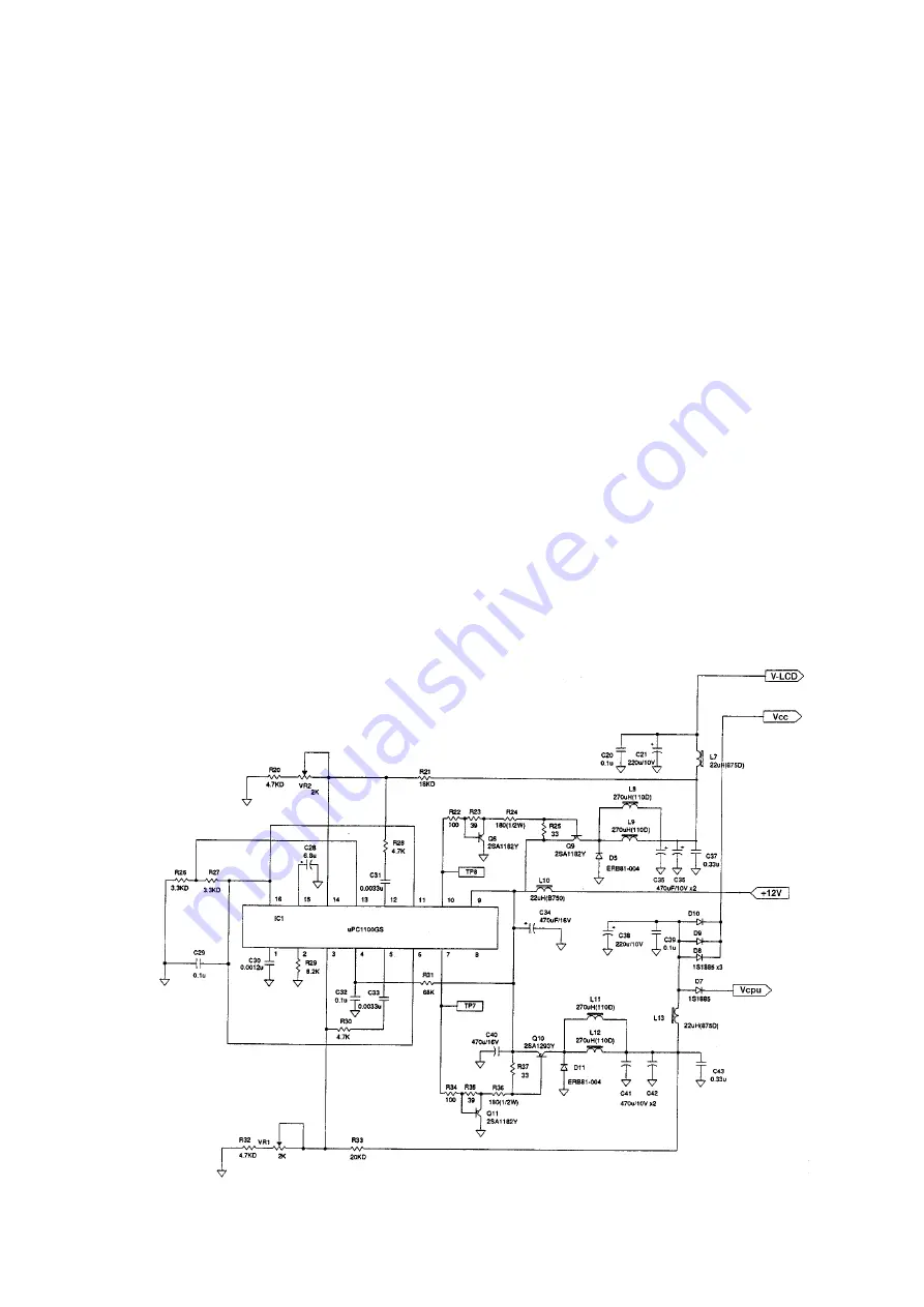
IC1 in Fig. 14 is a controller for a fixed frequency pulse width modulation(PWM) switching
regulator and has two constant voltage controllers. One controller is used to generate a 5V
power supply(V
CPU
,V
CC
) from the input power supply VIN(12VDC). The other one is for V
LCD
.
IC1 has a saw-tooth wave oscillator built in whose oscillating frequency is determined by
capacitor C30 connected to pin 1 and resister R29 connected to pin2. In this circuit
configuration, a saw-tooth wave of approx.75KHz is observed at pin 1 of IC1. Basically this saw-
tooth wave is compared with a control signal observed at pin5 of IC1. Only while the voltage
of the saw-tooth wave is lower than the control signal voltage, the period between pin 7 of IC1
is "L" becomes longer. As a result the period between external transistor Q11 and Q10 is
conductive becomes longer. The output voltage is fed back to pin 3 of IC1. An error amplifier
in IC1 makes a comparison between the half of the reference voltage and the feed-back signal
to pin 3 and generates a control signal(pin5 of IC1). As explained above the output voltage is
stabilized by the pulse width from pin 7, which is generated by comparing the control signal with
the saw-tooth wave.
V
CPU
is adjusted to 5.1V while V
CC
is 5V. This is done because the load on the V
CC
is greater than
the load on V
CPU
and the forward voltages of D8, D9, and D10 are higher than that of D7.The
voltage supplied to pin 6 of IC1 is called a dead time control signal. It controls the maximum
ON period of the output transistor in IC1. The maximum ON period is realized on IC1 by shorting
pin 6 and pin 16.
The saw-tooth wave oscillator of pin 1 of IC1 is used also for the control of this 5V power
supply(V
LCD
). The operation of the circuit is similar to that of the other 5V power supply(V
CPU
and
V
CC
). The output voltage is fed back to pin 14 of IC1. The control signal is produced using a
voltage generated by dividing the reference voltage inputted to pin 13 of IC1, and the feed back
signal. The output voltage is stabilized by the pulse width from pin 10, which is generated by
comparing the control signal with the saw-tooth wave. V
LCD
is adjusted to 5.0V with VR2.
Fig. 14 +5V Power(V
CC
,V
CPU
,V
LCD
) Circuit
Summary of Contents for QD-101MM
Page 39: ...38 6 CIRCUIT DIAGRAM PWB Fig 27 CIRCUIT DIAGRAM MAIN CIRCUIT No 1 ...
Page 40: ...39 Fig 27 CIRCUIT DIAGRAM MAIN CIRCUIT No 1 ...
Page 41: ...40 Fig 28 CIRCUIT DIAGRAM MAIN CIRCUIT No 2 ...
Page 42: ...41 Fig 28 CIRCUIT DIAGRAM MAIN CIRCUIT No 2 ...
Page 43: ...42 Fig 29 CIRCUIT DIAGRAM MAIN CIRCUIT No 3 ...
Page 44: ...43 Fig 29 CIRCUIT DIAGRAM MAIN CIRCUIT No 3 ...
Page 45: ...44 Fig 30 CIRCUIT DIAGRAM MAIN CIRCUIT No 4 ...
Page 46: ...45 Fig 30 CIRCUIT DIAGRAM MAIN CIRCUIT No 4 ...
Page 47: ...46 Fig 31 CIRCUIT DIAGRAM POWER CIRCUIT ...
Page 48: ...47 Fig 31 CIRCUIT DIAGRAM POWER CIRCUIT ...
Page 49: ...48 Fig 32 CIRCUIT DIAGRAM VIDEO CIRCUIT ...
Page 50: ...49 Fig 32 CIRCUIT DIAGRAM VIDEO CIRCUIT ...
Page 51: ...50 Fig 33 CIRCUIT DIAGRAM AUDIO CIRCUIT ...
Page 52: ...51 Fig 33 CIRCUIT DIAGRAM AUDIO CIRCUIT ...
Page 53: ...52 Fig 34 PWB PATTERN MAIN PWB FRONT SIDE ...
Page 54: ...53 Fig 34 PWB PATTERN MAIN PWB REAR SIDE ...
Page 66: ...PRINTED IN GERMANY ...


