


13
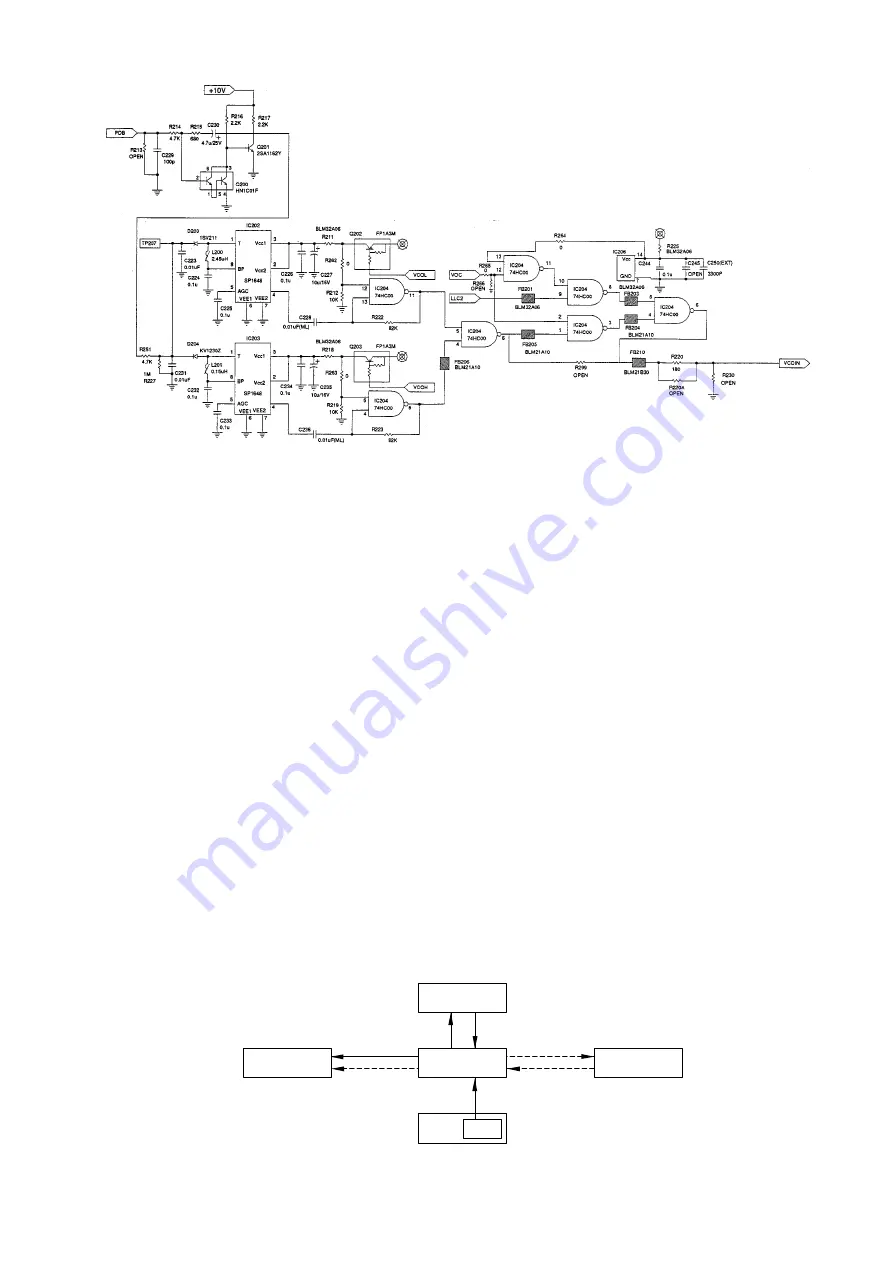
Fig.6 PLL Circuit
6. MEMORY CIRCUIT
BLOCK DIAGRAM is shown in Fig.2.
6.1.Field memory writing
When data sent from the signal selector is written into the field memory(IC103~105), FWCK
(clock slightly later than CLK) generated from the memory controller in IC100 is used.
6.2.Field memory reading
The clock (FRCK) and control signals which are generated in the field memory reading signal
generating circuit in IC100 are used to read data from the field memory.
Reading is asynchronous with writing. In the ordinary mode, data written into the field memory
are color-compensated and are sent to LCD.
In the enlargement mode, the enlargement control signal is sent to the field memory from the
field memory writing/reading signal generating circuit in IC100 to make the enlargement display
possible.
6.3.Menu, message display memory
The menu and message display is stored in the ROM area of IC400(MPU).
When the menu button is first pressed, MPU will write data and address into VRAM (IC108, 111)
via IC100. Moreover, VRAM data is read via IC100.
The data is sent to LCD at the timing of LCD.
Fig. 8 Memory Circuit Block Diagram
VRAM
IC100
ROM
MPU
LCD
FIELD MEMORY
menu and
message data
display data
IC108, 111
IC103~105
Summary of Contents for QD-101MM
Page 39: ...38 6 CIRCUIT DIAGRAM PWB Fig 27 CIRCUIT DIAGRAM MAIN CIRCUIT No 1 ...
Page 40: ...39 Fig 27 CIRCUIT DIAGRAM MAIN CIRCUIT No 1 ...
Page 41: ...40 Fig 28 CIRCUIT DIAGRAM MAIN CIRCUIT No 2 ...
Page 42: ...41 Fig 28 CIRCUIT DIAGRAM MAIN CIRCUIT No 2 ...
Page 43: ...42 Fig 29 CIRCUIT DIAGRAM MAIN CIRCUIT No 3 ...
Page 44: ...43 Fig 29 CIRCUIT DIAGRAM MAIN CIRCUIT No 3 ...
Page 45: ...44 Fig 30 CIRCUIT DIAGRAM MAIN CIRCUIT No 4 ...
Page 46: ...45 Fig 30 CIRCUIT DIAGRAM MAIN CIRCUIT No 4 ...
Page 47: ...46 Fig 31 CIRCUIT DIAGRAM POWER CIRCUIT ...
Page 48: ...47 Fig 31 CIRCUIT DIAGRAM POWER CIRCUIT ...
Page 49: ...48 Fig 32 CIRCUIT DIAGRAM VIDEO CIRCUIT ...
Page 50: ...49 Fig 32 CIRCUIT DIAGRAM VIDEO CIRCUIT ...
Page 51: ...50 Fig 33 CIRCUIT DIAGRAM AUDIO CIRCUIT ...
Page 52: ...51 Fig 33 CIRCUIT DIAGRAM AUDIO CIRCUIT ...
Page 53: ...52 Fig 34 PWB PATTERN MAIN PWB FRONT SIDE ...
Page 54: ...53 Fig 34 PWB PATTERN MAIN PWB REAR SIDE ...
Page 66: ...PRINTED IN GERMANY ...