17
8. LCD CONTROL CIRCUIT
LCD control signal is slower than the video signal of the computer. While the video signal is
serial data, the LCD display data is given as 4-bit parallel data for each RGB. In order to display
the bit signal of the computer in LCD, it is necessary to store the data of one screen in the
memory and read out the image data of one screen at the drive timing of LCD. To control them,
the field memory is controlled by the memory controller in IC100 as shown in the block diagram
in Fig. 2.
9. LCD UNIT
9.1.Interface signals
The shield case is connected to GND in LCD module.
(*1) The line mode(480 or 400 or 350) can be selected by the polarity of Hsync and Vsync.
(*2) Don't use "High".
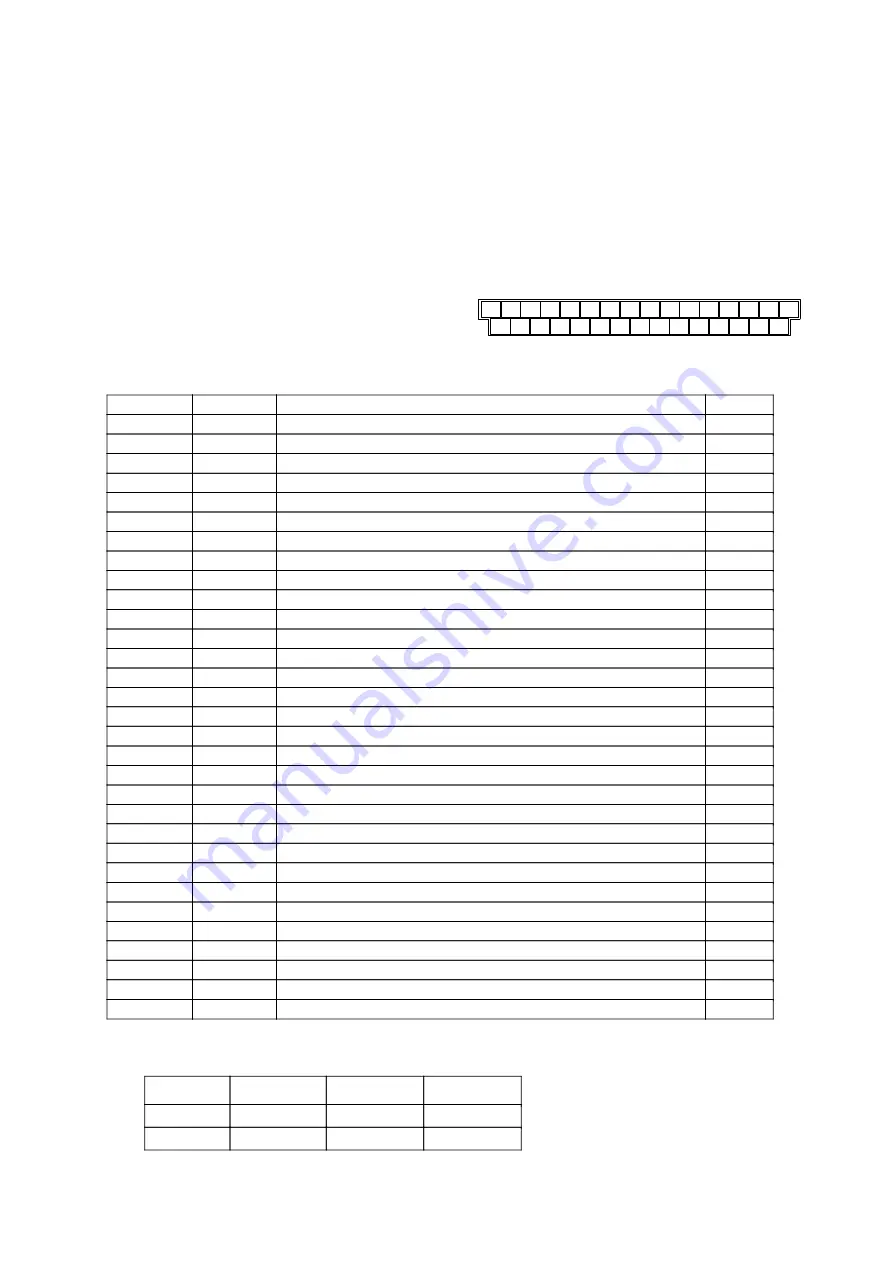
Table 4 Pin assignment of LCD unit
Pin
Code
Function
Remark
1
GND
2
CK
Sampling clock signal of data
3
Hsymc
Horizontally synchronous signal
(*1)
4
Vsync
Vertically synchronous signal
(*1)
5
GND
6
R0
Red data signal(LSB)
7
R1
Red data signal
8
R2
Red data signal
9
R3
Red data signal
10
R4
Red data signal
11
R5
Red data signal(MSB)
12
GND
13
G0
Green data signal(LSB)
14
G1
Green data signal
15
G2
Green data signal
16
G3
Green data signal
17
G4
Green data signal
18
G5
Green data signal(MSB)
19
GND
20
B0
Blue fata signal(LSB)
21
B1
Blue fata signal
22
B2
Blue fata signal
23
B3
Blue fata signal
24
B4
Blue fata signal
25
B5
Blue fata signal(MSB)
26
GND
27
ENAB
Data enable signal(Horizontal display position signal)
(*2)
28
Vcc
+5V power suppry
29
Vcc
+5V power suppry
30
TST
Open
31
TST
Open
CN1 Pin assignment
30
24
22
20
18
16
14
12
10
8
6
4
2
29
27
25
23
21
19
17
15
13
11
9
7
5
3
1
31
28
26
Mode
480line
400line
350line
Hsync
Negative
Negative
Positive
Vsync
Negative
Positive
Negative
Summary of Contents for QD-101MM
Page 39: ...38 6 CIRCUIT DIAGRAM PWB Fig 27 CIRCUIT DIAGRAM MAIN CIRCUIT No 1 ...
Page 40: ...39 Fig 27 CIRCUIT DIAGRAM MAIN CIRCUIT No 1 ...
Page 41: ...40 Fig 28 CIRCUIT DIAGRAM MAIN CIRCUIT No 2 ...
Page 42: ...41 Fig 28 CIRCUIT DIAGRAM MAIN CIRCUIT No 2 ...
Page 43: ...42 Fig 29 CIRCUIT DIAGRAM MAIN CIRCUIT No 3 ...
Page 44: ...43 Fig 29 CIRCUIT DIAGRAM MAIN CIRCUIT No 3 ...
Page 45: ...44 Fig 30 CIRCUIT DIAGRAM MAIN CIRCUIT No 4 ...
Page 46: ...45 Fig 30 CIRCUIT DIAGRAM MAIN CIRCUIT No 4 ...
Page 47: ...46 Fig 31 CIRCUIT DIAGRAM POWER CIRCUIT ...
Page 48: ...47 Fig 31 CIRCUIT DIAGRAM POWER CIRCUIT ...
Page 49: ...48 Fig 32 CIRCUIT DIAGRAM VIDEO CIRCUIT ...
Page 50: ...49 Fig 32 CIRCUIT DIAGRAM VIDEO CIRCUIT ...
Page 51: ...50 Fig 33 CIRCUIT DIAGRAM AUDIO CIRCUIT ...
Page 52: ...51 Fig 33 CIRCUIT DIAGRAM AUDIO CIRCUIT ...
Page 53: ...52 Fig 34 PWB PATTERN MAIN PWB FRONT SIDE ...
Page 54: ...53 Fig 34 PWB PATTERN MAIN PWB REAR SIDE ...
Page 66: ...PRINTED IN GERMANY ...


