


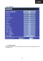


43
LC-32LD145
LC-39LD145
32
8.2 EN25QH16 16 Megabit Serial Flash Memory with 4Kbyte Uniform
Sector
8.2.1 General Description
The EN25QH16 is a 16 Megabit (2,048 K-byte) Serial Flash memory, with enhanced write
protection mechanisms. The EN25QH16 supports the standard Serial Peripheral Interface
(SPI), and a high performance Dual/Quad output as well as Dual/Quad I/O using SPI pins:
Serial Clock, Chip Select, Serial DQ0(DI), DQ1(DO), DQ2(WP#) and DQ3(HOLD#). SPI
clock frequencies of up to 80MHz are supported allowing equivalent clock rates of 160MHz
(80MHz x 2) for Dual Output and 320MHz (80MHz x 4) for Quad Output when using the
Dual/Quad I/O Fast Read instructions. The memory can be programmed 1 to 256 bytes at a
time, using the Page Program instruction. The EN25QH16 is designed to allow either single
Sector/Block at a time or full chip erase operation. The EN25QH16 can be configured to
protect part of the memory as the software protected mode. The device can sustain a
minimum of 100K program/erase cycles on each sector or block.
8.2.2 Features
Summary of Contents for LC-32LD145K
Page 12: ...12 LC 39LD145 LC 32LD145 English 21 Dimensional Drawings LC39LD145 ...
Page 15: ...15 LC 32LD145 LC 39LD145 3 Remove Speaker Wire 4 Remove AC Cord ...
Page 17: ...17 LC 32LD145 LC 39LD145 4 1 1 General Block Diagram 0 1 ...
Page 18: ...18 LC 39LD145 LC 32LD145 5 1 2 MB82 Placement of Blocks 0 2 ...
Page 21: ...21 LC 32LD145 LC 39LD145 ...
Page 22: ...22 LC 39LD145 LC 32LD145 ...
Page 23: ...23 LC 32LD145 LC 39LD145 ...
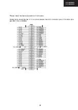
Page 24: ...24 LC 39LD145 LC 32LD145 11 2 4 Pinning ...
Page 25: ...25 LC 32LD145 LC 39LD145 ...
Page 26: ...26 LC 39LD145 LC 32LD145 14 TS4962M optional 2 5W ...
Page 35: ...35 LC 32LD145 LC 39LD145 ...
Page 36: ...36 LC 39LD145 LC 32LD145 ...
Page 38: ...38 LC 39LD145 LC 32LD145 27 x16 Package Pinout Top view 96ball FBGA Package ...
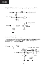
Page 39: ...39 LC 32LD145 LC 39LD145 28 7 SCALER AND LVDS SOCKETS 7 1 LVDS sockets Block Diagram ...
Page 41: ...41 LC 32LD145 LC 39LD145 30 8 1 2 Features 8 1 3 Block Diagram ...
Page 42: ...42 LC 39LD145 LC 32LD145 31 8 1 4 Pinning ...
Page 44: ...44 LC 39LD145 LC 32LD145 33 8 2 3 Block Diagram 8 2 4 Pinning ...
Page 45: ...45 LC 32LD145 LC 39LD145 34 ...
Page 48: ...48 LC 39LD145 LC 32LD145 37 10 3 VGA CN711 10 4 SCART SC1 ...
Page 51: ...51 LC 32LD145 LC 39LD145 11 3 Options Options 1 RET BACK RET BACK Options 2 ...
Page 52: ...52 LC 39LD145 LC 32LD145 11 5 Source Settings 11 4 Tuning Settings RET BACK ...
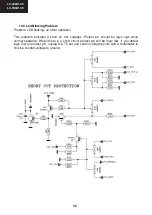
Page 79: ...79 LC 32LD145 LC 39LD145 POWER BOARD 17IPS20 39 1 2 ...
Page 80: ...80 LC 32LD145 LC 39LD145 POWER BOARD 17IPS20 39 2 2 ...
Page 107: ...107 LC 32LD145 LC 39LD145 ...


