40
LC-39LD145
LC-32LD145
29
7.2.
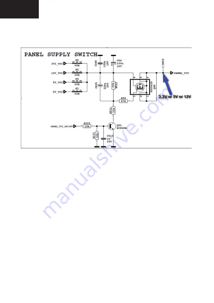
Panel Supply Switch Circuit
This switch is used to open and close panel supply of TCON. It is controlled by port of main
ucontroller. Also with this circit panel sequency could be adjusted correctly. 3 panel supplys
are connected to this circuit. All of them are optional according to panels.
8. SPI FLASH MEMORY
8.1
EN25Q64 64 Megabit Serial Flash Memory with 4Kbyte Uniform
Sector
8.1.1 General Description
The EN25Q64 is a 64 Megabit (8192K-byte) Serial Flash memory, with advanced write
protection mechanisms. The EN25Q64 supports the standard Serial Peripheral Interface
(SPI), and a high performance Dual output as well as Quad I/O using SPI pins: Serial
Clock, Chip Select, Serial DQ0(DI), DQ1(DO), DQ2(WP#) and DQ3(NC). SPI clock
frequencies of up to 50MHz are supported allowing equivalent clock rates of 100MHz for
Dual Output and 200MHz for Quad Output when using the Dual/Quad Output Fast Read
instructions. The memory can be programmed 1 to 256 bytes at a time, using the Page
Program instruction. The EN25Q64 is designed to allow either single Sector/Block at a time
or full chip erase operation. The EN25Q64 can be configured to protect part of the memory
as the software protected mode. The device can sustain a minimum of 100K program/erase
cycles on each sector or block.
Summary of Contents for LC-32LD145K
Page 12: ...12 LC 39LD145 LC 32LD145 English 21 Dimensional Drawings LC39LD145 ...
Page 15: ...15 LC 32LD145 LC 39LD145 3 Remove Speaker Wire 4 Remove AC Cord ...
Page 17: ...17 LC 32LD145 LC 39LD145 4 1 1 General Block Diagram 0 1 ...
Page 18: ...18 LC 39LD145 LC 32LD145 5 1 2 MB82 Placement of Blocks 0 2 ...
Page 21: ...21 LC 32LD145 LC 39LD145 ...
Page 22: ...22 LC 39LD145 LC 32LD145 ...
Page 23: ...23 LC 32LD145 LC 39LD145 ...
Page 24: ...24 LC 39LD145 LC 32LD145 11 2 4 Pinning ...
Page 25: ...25 LC 32LD145 LC 39LD145 ...
Page 26: ...26 LC 39LD145 LC 32LD145 14 TS4962M optional 2 5W ...
Page 35: ...35 LC 32LD145 LC 39LD145 ...
Page 36: ...36 LC 39LD145 LC 32LD145 ...
Page 38: ...38 LC 39LD145 LC 32LD145 27 x16 Package Pinout Top view 96ball FBGA Package ...
Page 39: ...39 LC 32LD145 LC 39LD145 28 7 SCALER AND LVDS SOCKETS 7 1 LVDS sockets Block Diagram ...
Page 41: ...41 LC 32LD145 LC 39LD145 30 8 1 2 Features 8 1 3 Block Diagram ...
Page 42: ...42 LC 39LD145 LC 32LD145 31 8 1 4 Pinning ...
Page 44: ...44 LC 39LD145 LC 32LD145 33 8 2 3 Block Diagram 8 2 4 Pinning ...
Page 45: ...45 LC 32LD145 LC 39LD145 34 ...
Page 48: ...48 LC 39LD145 LC 32LD145 37 10 3 VGA CN711 10 4 SCART SC1 ...
Page 51: ...51 LC 32LD145 LC 39LD145 11 3 Options Options 1 RET BACK RET BACK Options 2 ...
Page 52: ...52 LC 39LD145 LC 32LD145 11 5 Source Settings 11 4 Tuning Settings RET BACK ...
Page 79: ...79 LC 32LD145 LC 39LD145 POWER BOARD 17IPS20 39 1 2 ...
Page 80: ...80 LC 32LD145 LC 39LD145 POWER BOARD 17IPS20 39 2 2 ...
Page 107: ...107 LC 32LD145 LC 39LD145 ...


