20
LC-39LD145
LC-32LD145
7
2. AUDIO AMPLIFIER STAGE
TAS5721 (optional)
2.1. General Description
The TAS5721 is a 15-W stereo or 2x10 W + 1x15 W2.1 device, efficient, digital audio-power
amplifier fordriving stereo bridge-tied speakers. One serial datainput allows processing of
up to two discrete audiochannels and seamless integration to most digitalaudio processors
and MPEG decoders. The deviceaccepts a wide range of input data and data rates. Afully
programmable data path routes these channelsto the internal speaker drivers.The TAS5721
is a slave-only device receiving allclocks from external sources. The TAS5721 operateswith
a PWM carrier between a 384-kHz switching rateand a 352-KHz switching rate, depending
on the inputsample rate. Oversampling combined with a fourth- order noise shaper provides
a flat noise floorand excellent dynamic range from 20 Hz to 20 kHz.
2.2. Features
• Audio Input/Output
– 15Wx2 into 8
– Supports Single Device 0.1, 2.0, 2.1 Modes
– Wide PVDD Range, From 4.5 V to 26 V Performance
– Efficient Class-D Operation Eliminates Need for Heatsinks
– Requires Only 3.3 V and PVDD
– One Serial Audio Input (Two Audio Channels)
– I2C Address Selection via PIN (Chip Select)
– Supports 8-kHz to 48-kHz Sample Rate (LJ/RJ/I2S)
– External Headphone-Amplifier Shutdown Signal
– Integrated CAP-Free Headphone Amplifier
– Stereo Headphone (Stereo 2-V RMS Line Driver) Outputs
• Audio/PWM Processing
– Independent Channel Volume Controls With The 24-dB to Mute
– Separate Dynamic Range Control for Satellite and Sub Channels
– 21 Programmable Biquads for Speaker EQ
– Programmable Coefficients for DRC Filters
– DC Blocking Filters
– Support for 3D Effects
• General Features
– Serial Control Interface Operational Without MCLK
– Factory-Trimmed Internal Oscillator for Automatic Rate Detection
– Surface Mount, 48-Pin, 7-mm × 7-mm HTQFP Package
– Thermal and Short-Circuit Protection
1
Summary of Contents for LC-32LD145K
Page 12: ...12 LC 39LD145 LC 32LD145 English 21 Dimensional Drawings LC39LD145 ...
Page 15: ...15 LC 32LD145 LC 39LD145 3 Remove Speaker Wire 4 Remove AC Cord ...
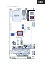
Page 17: ...17 LC 32LD145 LC 39LD145 4 1 1 General Block Diagram 0 1 ...
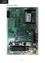
Page 18: ...18 LC 39LD145 LC 32LD145 5 1 2 MB82 Placement of Blocks 0 2 ...
Page 21: ...21 LC 32LD145 LC 39LD145 ...
Page 22: ...22 LC 39LD145 LC 32LD145 ...
Page 23: ...23 LC 32LD145 LC 39LD145 ...
Page 24: ...24 LC 39LD145 LC 32LD145 11 2 4 Pinning ...
Page 25: ...25 LC 32LD145 LC 39LD145 ...
Page 26: ...26 LC 39LD145 LC 32LD145 14 TS4962M optional 2 5W ...
Page 35: ...35 LC 32LD145 LC 39LD145 ...
Page 36: ...36 LC 39LD145 LC 32LD145 ...
Page 38: ...38 LC 39LD145 LC 32LD145 27 x16 Package Pinout Top view 96ball FBGA Package ...
Page 39: ...39 LC 32LD145 LC 39LD145 28 7 SCALER AND LVDS SOCKETS 7 1 LVDS sockets Block Diagram ...
Page 41: ...41 LC 32LD145 LC 39LD145 30 8 1 2 Features 8 1 3 Block Diagram ...
Page 42: ...42 LC 39LD145 LC 32LD145 31 8 1 4 Pinning ...
Page 44: ...44 LC 39LD145 LC 32LD145 33 8 2 3 Block Diagram 8 2 4 Pinning ...
Page 45: ...45 LC 32LD145 LC 39LD145 34 ...
Page 48: ...48 LC 39LD145 LC 32LD145 37 10 3 VGA CN711 10 4 SCART SC1 ...
Page 51: ...51 LC 32LD145 LC 39LD145 11 3 Options Options 1 RET BACK RET BACK Options 2 ...
Page 52: ...52 LC 39LD145 LC 32LD145 11 5 Source Settings 11 4 Tuning Settings RET BACK ...
Page 79: ...79 LC 32LD145 LC 39LD145 POWER BOARD 17IPS20 39 1 2 ...
Page 80: ...80 LC 32LD145 LC 39LD145 POWER BOARD 17IPS20 39 2 2 ...
Page 107: ...107 LC 32LD145 LC 39LD145 ...


