background image

LC-42AD5E/RU/S

ii

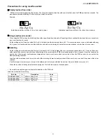
Precautions for using lead-free solder

„

Employing lead-free solder

• “PWBs” of this model employs lead-free solder. The LF symbol indicates lead-free solder, and is attached on the PWBs and service manuals. The

alphabetical character following LF shows the type of lead-free solder. 

Example:

„

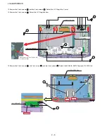
Using lead-free wire solder

• When fixing the PWB soldered with the lead-free solder, apply lead-free wire solder. Repairing with conventional lead wire solder may cause dam-

age or accident due to cracks.

As the melting point of lead-free solder (Sn-Ag-Cu) is higher than the lead wire solder by 40 

°

C, we recommend you to use a dedicated soldering

bit, if you are not familiar with how to obtain lead-free wire solder or soldering bit, contact our service station or service branch in your area.

„

Soldering

• As the melting point of lead-free solder (Sn-Ag-Cu) is about 220 

°

C which is higher than the conventional lead solder by 40 

°

C, and as it has poor

solder wettability, you may be apt to keep the soldering bit in contact with the PWB for extended period of time. However, Since the land may be
peeled off or the maximum heat-resistance temperature of parts may be exceeded, remove the bit from the PWB as soon as you confirm the
steady soldering condition.

Lead-free solder contains more tin, and the end of the soldering bit may be easily corroded. Make sure to turn on and off the power of the bit as
required.

If a different type of solder stays on the tip of the soldering bit, it is alloyed with lead-free solder. Clean the bit after every use of it.

When the tip of the soldering bit is blackened during use, file it with steel wool or fine sandpaper.

• Be careful when replacing parts with polarity indication on the PWB silk.

Lead-free wire solder for servicing

L

F a

Indicates lead-free solder of tin, silver and copper.

L

F a/a

Indicates lead-free solder of tin, silver and copper.

Part No.

Description

Code

ZHNDAi123250E

J

φ

0.3mm  250g (1roll) 

BL

ZHNDAi126500E

J

φ

0.6mm  500g (1roll)

BK

ZHNDAi12801KE

J

φ

1.0mm  1kg (1roll)

BM

Summary of Contents for AQUOS LC-42AD5E

Page 1: ...alization to factory settings 3 21 10 Lamp error detection 3 21 11 Public Mode Hotel Mode 3 22 CHAPTER 4 TROUBLESHOOTING TABLE 1 TROBLESHOOTING TABLE 4 1 CHAPTER 5 MAJOR IC INFORMATIONS 1 MAJOR IC INFORMATIONS 5 1 CHAPTER 6 OVERALL WIRING DIAGRAM BLOCK DIAGRAM 1 OVERALL WIRING DIAGRAM 6 1 2 SYSTEM BLOCK DIAGRAM 6 2 3 MAIN BLOCK DIAGRAM 6 3 4 POWER BLOCK DIAGRAM 6 4 CHAPTER 7 PRINTED WIRING BOARD 1...

Page 2: ...e AC voltage drop across the resistor All checks must be repeated with the AC cord plug connection reversed If necessary a nonpolarized adaptor plug must be used only for the purpose of completing these checks Any reading of 1 05 V peak this corresponds to 0 7 mA peak AC or more is excessive and indicates a potential shock hazard which must be corrected before returning the monitor to the owner SA...

Page 3: ...l lead solder by 40 C and as it has poor solder wettability you may be apt to keep the soldering bit in contact with the PWB for extended period of time However Since the land may be peeled off or the maximum heat resistance temperature of parts may be exceeded remove the bit from the PWB as soon as you confirm the steady soldering condition Lead free solder contains more tin and the end of the so...

Page 4: ...LC 42AD5E RU S 1 1 LC 42AD5EB Service Manual CHAPTER 1 OPERATION MANUAL 1 SPECIFICATIONS ...

Page 5: ...LC 42AD5E RU S 1 2 2 OPERATION MANUAL ...

Page 6: ...LC 42AD5E RU S 1 3 ...

Page 7: ...LC 42AD5E RU S 1 4 ...

Page 8: ...LC 42AD5E RU S 1 5 ...

Page 9: ...LC 42AD5E RU S 1 6 ...

Page 10: ...LC 42AD5E RU S 1 7 3 DIMENSIONS Unit mm ...

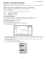
Page 11: ... PARTS 1 REMOVING OF MAJOR PARTS 1 Remove the 2 lock screws 10 lock screws and the 4 lock screws Detach the Rear Cabinet 2 Remove the 4 lock screws Detach the Stand Assist 3 Remove the 2 lock screws Detach the Bottom Cover 1 2 3 1 2 3 4 5 BOTTOM COVER STAND ASSIST ANGLE 4 5 ...

Page 12: ... S 2 2 4 Remove the 4 lock screws Detach the Center Angle 5 Remove the 2 lock screws Detach the Stand Fix Angle 6 Remove the 4 lock screws Detach the Stand Angle 6 7 STAND FIX ANGLE CENTER ANGLE 6 7 8 STAND ANGLE 8 ...

Page 13: ...LC 42AD5E RU S 2 3 7 Remove the 4 lock screws Detach the Speaker Unit 8 Remove all the connectors from PWBs 9 SPEAKER 9 FOR Wire RA Wire RA Wire RA to Pin Wire RA Wire RA to WH x7 for RA w ire ...

Page 14: ... 2 4 9 Remove all the connectors from PWBs 10 Remove the 5 lock screws Detach the Chassis Tray Unit Wire LA Wire LC Wire LC Wire LA Wire LA LD to WH x5 10 Wire LV Red Wire Blue Wire Wire LV to WH Chassis Tray Unit 10 ...

Page 15: ...LC 42AD5E RU S 2 5 11 Remove the 2 lock screws and the 1 screw Detach the Tuner Unit 12 Remove the 4 lock screws 11 12 Chassis Tray Unit Tuner Unit B to B connector 11 12 13 Center Left Right Center 13 ...

Page 16: ...ws Detach the LCD Angle Bottom 15 Remove the 2 lock screws the 1 lock screw and the 2 lock screws Detach the 42WXGA SMPL Panel and R C LED Unit 14 15 16 LCD ANG TOP CEN KS LCD ANG BTM TRAY ANG Place hole on convex of TRAY ANG to hexagonal pillar 15 16 14 16 17 18 19 42WXGA SMPL PNL R C LED UNIT Wire RA Shorter Longer 19 17 18 ...

Page 17: ...e 1 RS 232C Method Description HyperTerminal The hardware tools requirement are 1 A Modem null Cross type DB9 female to DB9 female cable 2 An adaptor DB9 male to mini Din 9 pin male cable Sharp Code QCNWGA015WJPZ 3 Make the connections as indicated in the figure Before using RS 232C updating method is necessary to configure a Terminal PC software HyperTerminal has been selected as a Terminal soft ...

Page 18: ...me P55_115200bps 8 Select a the same COM port used in item 2 and select the Port Settings properties as follows 9 Select the same General and ASCII properties as item 3 10 Close HyperTerminal session answering Yes to close current connection and Yes to save session P55_115200bps To start updating session click over P55_9600bps icon that you can find in the START All programs Accessories Communicat...

Page 19: ...s Communications HyperTerminal HyperTerminal folder 4 Using Transfer Send file menu select desired file bin format and the transmission protocol Xmodem as show below 5 After press Send button the updating process starts as follows 6 When flash update process finishes the Flash Programming Complete label appears in the screen the device automatically go to switch off and in a few seconds go to swit...

Page 20: ...o jp authors VA002416 teraterm html The address may be changed in future Tera Term Pro supported operating systems MS Windows 95 or upper MS Windows NT 3 5 and 4 0 or upper Note For Windows 3 1 use Tera Term version 1 X Copy all the distribution files to an empty floppy disk or temporary directory for example C TEMP Run SETUP EXE and follow the instruction given by it After the installation the di...

Page 21: ...LC 42AD5E RU S 3 5 1 Select Serial COM X O K 2 Select Terminal 3 Choose the same options as the above picture ...

Page 22: ...ing a wrong command as for example aaa TV set returns an err label as an syntaxes ERROR Not correct order or sequence Send a DWMD capital letters command to enter TV set in Download Mode Change a baud rate to 115200 Select Setup Baud rate 115200 O K Serial port to use COM x Baud rate 9600 Data 8 bits Parity none Stop 1 bit Flow control none Enter O K ...

Page 23: ...LC 42AD5E RU S 3 7 7 Select File Transfer XMODEM Sent 8 Choose the file for upgrade and click Open 9 After select Open the upgrade process starts as follows ...

Page 24: ...he TV set 3 How to update the Digital Board Software There are 2 methods to update the Digital Board Software on Flash Memory IC4203 thought the Digital Processor IC4001 Jig RS 232 Method From PC trough RS 232C COM port PCMCIA CARD Compact Flash Memory Method NOTE The PCMCIA method is only compatible with those PCs running XP Windows Version 3 1 Jig RS 232 Method Description Hardware requirements ...

Page 25: ...st suitable RS232 Serial Port from Port Setting Process Menu 3 Select the following settings from Port Settings Menu Bits Per Second 115200 Parity None Data bits 8 Stop bits 1 Hardware Flow Control OFF Procedure for updating the TV set 1 Switch off the TV set to be updated in DTV mode 2 Start Winupload It will appear the following picture on PC ...

Page 26: ...and open the urt data file from data directory NOTE Consider the version shown below just an example may be is not the latest one and could be different depending on the TV set destination market Country or model 6 Switch On the TV Set previously in DTV Mode The Uploading Process starts automatically ...

Page 27: ... the full uploading process is finished in the Winupload window appears the label Preparing to start application for a new TV Set and just now in the TV screen of the updated set appears a congratulations label Item 8 NOTE Do not turn off the TV set while the software updating was in progress 7 Unplug the AC cord 8 Disconnect the Jig from TV Set Software Version verification procedure 1 Connect th...

Page 28: ...are the CF Card using the Storage Media Manager 1 0 1 SMM 1 Insert PCMCIA Compact Flash CF CF Adapter 2 Execute SMM If SMM does not appear or a Windows Error Box appears please verify there are no USB media drives connected to the PC NOTE Consider that it s recommended remove unnecessary media during SMM execution Probably If you try to use an USB Multi Card Reader with SMM doesn t work fine 3 If ...

Page 29: ...p Menu please format the Drive 5 Formatting the CF card Select Yes to confirm the action NOTE All FC s data of the inside are erased 6 If SMM formatted card already appears under SHARP DRIVES box please continue if not try to repeat from item 1 Select origin folder and img data file to be written in the CF card ...

Page 30: ...14 7 First of all select copy target drive and then use Drag drop for the img file 8 Wait copy is in process 9 Copy is finished when the Copying progress bar disappears and the name of data file appears in the File Box ...

Page 31: ...ff the LCD TV Set in DTV mode 2 Insert PCMCIA Card already prepared according the details before given at How to prepare the CF Card using the Storage Media Manager 1 0 1 SMM 3 Switch On the LCD TV Set it starts automatically the updating Items 1 to 4 4 Wait till the finishing indication is shown 5 For checking the correct update please Select DTV Menu on TV Set The following On Screen Display wil...

Page 32: ...tion of display in adjustment process mode 1 key operation Input mode is switched automatically when relevant adjustment is started so far as the necessary input signal is available 2 Description of display Caution Use due care in handling the information described here lest the users should know how to enter the adjustment process mode If the settings are tampered with in this mode unrecoverable ...

Page 33: ...TUNER ADJ ENTER PAL TUNER auto adjustment execution 3 PAL ADJ ENTER PAL auto adjustment execution 4 TUNER ADJ ENTER TUNER auto adjustment execution 5 CONTRAST SD 32 PAL contrast adjustment 6 SECAM CB OFFSET 1 SECAM offset adjustment 7 SECAM CR OFFSET 1 SECAM offset adjustment 8 TUNER A DAC 32 TUNER DAC adjustment 9 RF AGC 16 RF AGC adjustment 4 11 COMP 15K 1 COMP 15K ADJ ENTER COMP15K auto adjustm...

Page 34: ...adjustment gradation 4G adjustment value 3 M GAMMA B 4 0 W B adjustment gradation 4B adjustment value 4 M GAMMA R 5 0 W B adjustment gradation 5R adjustment value 5 M GAMMA G 5 0 W B adjustment gradation 5G adjustment value 6 M GAMMA B 5 0 W B adjustment gradation 5B adjustment value 7 M GAMMA R 6 0 W B adjustment gradation 6R adjustment value 8 M GAMMA G 6 0 W B adjustment gradation 6G adjustment...

Page 35: ...it Field Colour Bar RF signal UV Terminal TUNER Feed the PAL Sprit Field colour bar signal to TUNER Signal level 55 dB µV 1dB 1dB 75Ω LOAD 2 Auto adjustment performance Adjustment process Page3 Bring the cursor on RF AGC ADJ and press OK RF AGC ADJ OK appears when finished Adjustment point Adjustment Conditions Adjustment procedure 1 Setting Signal PAL Full Field Colour Bar RF signal Feed the RF s...

Page 36: ...nge G When G is lowered the weaker of R and B must be fixed 4 If G is changed in step 3 change the values of M GAMMA G1 M GAMMA G5 on pages 8 11 and 9 11 of process adjustment as follows When not changed go to step5 Offset value of M GAMMA G1 Offset value of M GAMMA G6 160 960 Offset value of M GAMMA G2 Offset value of M GAMMA G6 320 960 Offset value of M GAMMA G3 Offset value of M GAMMA G6 480 96...

Page 37: ...ist After confirming that the lamp error counter has been erased select STAND BY CAUSE RESET on point 3 page 10 11 of the adjustment process and select ON using the right cursor For execute press OK in the R C and the label OK appears on Screen Caution When the factory settings have been made all user setting data including the channel settings are initialized The adjustments done in the adjustmen...

Page 38: ...to set the maximum volume at limited level 3 VOLUME FIXED VARIABLE FIXED Is possible to fix the sound volume at limited level When FIXED is selected the sound volume before limited is fixed 4 VOLUME FIXED LEVEL 0 60 If FIXED has been selected is possible to set a fixed volume at the level that is chosen 5 RC BUTTON RESPOND NO RESPOND If NO RESPOND is selected the remote control keys are inoperativ...

Page 39: ...03 D7803 etc YES Check voltage of Emitter Q7902 Does it equal to 15V NO Check IC7901 R7920 R7921 Q7901 YES Is BU5V PA pin20 and pin21 output 5V Is UR5V PA pin10 15 output 5V NO Check IC7901 Q7901 D7951 R7950 R7951 R7961 L7951 IC7952 etc YES Is P CON1 PB pin1 signal normaly NO Check PB pin1 Q7272 Q7240 Q7241 Q7311 etc YES Is P CON2 PB pin2 signal normaly NO Check PB pin2 Q7309 IC7304 Q7903 etc YES ...

Page 40: ...MUTE on the remote control Set the desired volume 2 Are headphones connected to HEADPHONE J1301 Disconnect them 3 Is ANT CABLE disconnected or connected improperly Connect it correctly as per the operation manual NO Refer to No sound output in all modes NO Is the SIF signal SIF_IN sent to pin 31 of IC3002 VCT YES Check whether 5V and 8V are supplied to pins 33 and 18 of IC3002 respectively Or chec...

Page 41: ...2 terminal J1101 to pin 11 of IC3002 VCT YES Refer to No sound output in all modes No sound from external input devices 3 No sound from an external input device connected to EXT3 EXT3 Is IN3 L audio signal sent from pin 3 of J1201 terminal to pin 16 of IC3002 VCT NO Check pins 3 and 5 of EXT3 J1201 and connection to an external input device Is IN3 R audio signal sent from pin 5 of J1201 terminal t...

Page 42: ... Is HDMI L audio signal sent from J2701 terminal to pin 14 of IC2704 SW NO Check the line between J2701 and IC2704 Q2704 Q2705 etc Is HDMI R audio signal sent from J2701 terminal to pin 5 of IC2704 SW YES Is HDMI L audio signal sent to pins 10 of IC3002 Is HDMI R audio signal sent to pins 9 of IC3002 NO Check the line between IC2704 and IC3002 YES Refer to No sound output in all modes ...

Page 43: ...ns 24 L ch and 23 R ch of IC3002 to pins 3 L ch and 1 R ch of EXT1 Q1108 Q1107 etc No sound except from speakers 2 No audio output from EXT2 SCART terminal Checklist 1 Is the MUTE button on the remote control set to ON Set to OFF 2 Check the connection to external devices Is there any improper connection Is audio signal sent to pins 24 L ch and 22 R ch of EXT2 J1101 YES Check the connection to EXT...

Page 44: ...rcuits and S MUTE line Q1204 Q1203 etc NO Is audio signal sent from pins 22 L ch and 21 R ch of IC3002 NO Check IC3002 or peripheral circuits YES Check the audio signal output line from pins 22 L ch and 21 R ch of IC3002 to pins 13 L ch and 15 R ch of AUDIO_OUTPUT Q1202 Q1201 etc DTV troubleshooting The unit does not enter the DTV mode Or the DTV menu does not appear YES Go to The unit does not en...

Page 45: ...heral circuits of X4001 X4002 D TUNER UNIT YES Does each REG IC206 REG IC208 REG and IC205 REG driving IC202 work normally NO Check peripheral circuits of IC206 IC208 IC205 YES Is a voltage applied to pin 20 I2CSEL of P202 High 3 3V NO MAIN UNIT Check around the pin 1 of IC1710 YES Is FESCL FESDA signal sent to pins 22 and 21 of P202 and pins 1 and 13 of IC204 SW NO Check peripheral circuits of IC...

Page 46: ...05 and its peripheral circuits YES Are video signals R G B CVBS fed from pins 179 180 181 and 184 of IC3002 NO Check peripheral circuits of IC3002 YES Are scrambled images not displayed YES DIGITAL UNIT Check 5V output of pin 1 2 5 and 6 of IC4702 Check 5V of pin 6 of Q4401 NO Refer to No video output in all modes No audio output during DTV reception Sound is low DIGITAL UNIT Is audio signal fed t...

Page 47: ... 1 Is INPUT SOURCE button on the remote control set up correctly See the operation manual and set INPUT SOURCE to TV 2 Is MENU PICTURE Contrast Brightness set to MIN Set it to an appropriate level 3 Is ANT CABLE disconnected or connected improperly Connect it correctly as per the operation manual Is level of pins 15 and 14 of tuner TU201 and pins 10 and 11 of IC201 IF DEMOD at H NO These are commu...

Page 48: ...S Is composite video signal VIN1 sent to input terminal pin 190 of IC3002 VCT NO Check IC2702 SW and peripheral circuits YES Refer to No video output in all modes When EXT1 is used for external input No picture on the display 4 No EXT1 RGB output of the external input system Checklist 1 Is INPUT SOURCE button on the remote control set up correctly See the operation manual and set INPUT SOURCE to E...

Page 49: ...its YES Refer to No video output in all modes When EXT2 is used for external input No picture on the display 6 No EXT2 Composite output of the external input system Checklist 1 Is INPUT SOURCE button on the remote control set up correctly See the operation manual and set INPUT SOURCE to EXIT2 2 Is MENU PICTURE CONTRAST BRIGHTNESS set to MIN Set it to an appropriate level 3 Check the connection to ...

Page 50: ...of IC3002 VCT NO Check CONNECTOR P1102 SC2703 SCART2 J1101 and peripheral circuits YES Refer to No video output in all modes When EXT2 is used for external input No picture on the display 8 No EXT2 Y C output of the external input system Checklist 1 Is INPUT SOURCE button on the remote control set up correctly See the operation manual and set INPUT SOURCE to EXIT2 2 Is MENU PICTURE CONTRAST BRIGHT...

Page 51: ...VIN7 sent to input termi nal pin 184 of IC3002 VCT NO Check IC2705 SW and peripheral circuits YES Refer to No video output in all modes When EXT3 is used for external input No picture on the display 10 No EXT3 Y C output of the external input system Checklist 1 Is INPUT SOURCE button on the remote control set up correctly See the operation manual and set INPUT SOURCE to EXIT3 2 Is MENU PICTURE CON...

Page 52: ...vel 3 Check the connection to the external device Connect it correctly as per the operation manual for the device Is EXT4 selected with INPUT SOURCE button on the remote control NO Select EXT4 with INPUT SOURCE button on the remote con trol YES Is D SUB COMPONENT signal PCV_R G B sent to pins 1 2 and 3 of EXT4 TERMINAL SC2303 NO Check D SUB adaptor and external connection YES Is D SUB COMPONENT si...

Page 53: ...rol YES Is the type of video signal Signal Type from HDMI connected external device set NO From MENU Option HDMI Setup Signal Type select a signal type RGB YCbCr 4 4 4 or YCbCr 4 2 2 YES Is the type of color signal Color Matrix from HDMI connected external device set NO From Option HDMI Setup Color Matrix select a color signal type ITU601 or ITU709 YES Is TMDS data RX signal sent to pins 1 12 of E...

Page 54: ...l YES Is the type of video signal Signal Type from HDMI connected external device set NO From MENU Option HDMI Setup Signal Type select a signal type RGB YCbCr 4 4 4 or YCbCr 4 2 2 YES Is the type of color signal Color Matrix from HDMI connected external device set NO From Option HDMI Setup Color Matrix select a color signal type AUTO ITU601 or ITU709 YES Is TMDS data RX signal sent to pins 1 12 o...

Page 55: ... the monitor refer to No picture for each terminal 6 The video output from EXT1 is not the monitor output output of the picture now watching The picture of the last selected TV channel is always sent to EXT1 Specification Is video signal sent to pin 19 of SCART1 J1101 YES Check SCART1 external connection or input setting NO Is video signal V OUT1 sent from pin 2 of IC1102 SW YES Check SCART1 J1101...

Page 56: ...t signal is not sent to the monitor 5 When the monitor picture is not sent and is not displayed on the monitor refer to No picture for each terminal 6 The video output from EXT1 is not the monitor output output of the picture now watching The picture of the last selected TV channel is always sent to EXT1 Specification Is video signal sent to pin 40 of SCART2 J1101 YES Check SCART2 external connect...

Page 57: ... No picture for each terminal 6 The video output from EXT1 is not the monitor output output of the picture now watching The picture of the last selected TV channel is always sent to EXT1 Specification Is video signal sent to pin 40 of SCART2 J1101 YES Check SCART2 external connection or input setting NO Is video signal V OUT2 sent from pin 2 of IC1101 SW YES Check SCART2 J1101 and peripheral circu...

Page 58: ...Programmable Gate Arrays for signal selector and synchronous processing of each digitalized input signal This IC functions as extended I O of the main microcontroller and controls timing of bus signals among ICs etc 1 6 IC1905 VHiSii9025 1Q The Sii9025 is a compliant with the latest HDMI 1 2 High Definition Multimedia Interface specification Backward compatibility with DVI 1 0 allows HDMI systems ...

Page 59: ...for the CPU with a built in digital processor and application software have been written on this Flash Memory The digital processor reads these soft wares on start up and implements them 1 9 IC4201 4202 RH iXB742WJZZQ This IC is 64Mb SDRAM static dynamic random access memory IC In this equipment it is used for SMI memory for image processing and data is used for operation of the digital processor ...

Page 60: ...nput for capacitor 7 DGND Digital ground 8 AUD O Audio output 9 TOP Tuner AGC TakeOver Point TOP 10 SDA I O I2C bus data input output 11 SCL I I2C bus clock input 12 SIOMAD O Sound intercarrier output and MAD select 13 N C Not connected 14 TAGC O TAGC14tuner AGC output 15 REF I 4MHz crystal or reference input 16 VAGC VIF AGC for capacitor 17 CVBS O Video output 18 AGND Analog ground 19 VPLL VIF PL...

Page 61: ...data bit 7 42 D6 O Parallel MPEG data bit 6 40 D5 O Parallel MPEG data bit 5 39 D4 O Parallel MPEG data bit 4 37 D3 O Parallel MPEG data bit 3 36 D2 O Parallel MPEG data bit 2 35 D1 O Parallel MPEG data bit 1 33 D0 O Parallel MPEG data bit 0 44 CLK_OUT O MPEG byte or bit clock 46 STR_OUT O MPEG first byte sync 47 D NOT_P O MPEG data valid parity 48 ERROR O MPEG packet error Front end controls 18 A...

Page 62: ...LC 42AD5E RU S 5 5 2 3 IC301 IC302 VHiTDA8931T 1Y 2 3 1 Block Diagram ...

Page 63: ...ference ground for pins POWERUP ENABLE and DIAG 10 VSSD Negative digital supply voltage heat spreader 11 VSSD Negative digital supply voltage heat spreader 12 OVP Overvoltage protection reference input 13 HVP Half supply voltage output for charging SE capacitor 14 STABI Decoupling of internal stabilizer 15 VSSP Negative power supply voltage 16 OUT PWM output 17 BOOT Bootstrap capacitor connection ...

Page 64: ...121 ODCK O Output Data Clock Digital Audio Output Pins 97 XTALIN I Crystal Clock Input 96 XTALOUT O Crystal Clock Output 88 MCLKOUT O Audio Master Clock Output 86 SCK O I2S Serial Clock Output 85 WS O I2S Word Select Output 84 SD0 O I2S Serial Data Output 78 SPDIF O S PDIF Audio Output 77 MUTEOUT O Mute Audio Output Configuration Programming Pins 104 INT O Interrupt Output 102 RESET I Reset Pin Ac...

Page 65: ... 48 R0X1 I HDMI Port 0 TMDS input data pair 47 R0X1 I 52 R0X2 I HDMI Port 0 TMDS input data pair 51 R0X2 I 59 R1XC I HDMI Port 1 TMDS input clock pair 58 R1XC I 63 R1X0 I HDMI Port 1 TMDS input data pair 62 R1X0 I 67 R1X1 I HDMI Port 1 TMDS input data pair 66 R1X1 I 71 R1X2 I HDMI Port 1 TMDS input data pair 70 R1X2 I Power and Ground Pins 22 23 35 74 79 92 105 114 128 139 CVCC18 Digital Logic VCC...

Page 66: ... Left 27 SPEAKERR O Analog Loudspeaker Output Right 28 SPEAKERL O Analog Loudspeaker Output Left 29 SUBWOOFER TEST O I Analog SUBWOOFER Output Test Input 30 VREFSIF Reference Voltage Audio SIF 31 SIFIN I Differential Sound IF Input 32 SIFIN I Differential Sound IF Input 33 VSUP5 0 Supply Voltage Analog 5 0 V 34 GNDA Ground Analog Platform Ground 35 GND3 3DIG Ground Digital Interfaces 36 VSUP3 3DIG...

Page 67: ...ut Output Test point 94 OSDH I O Graphic Horizontal Sync Input Output Test point 95 GND3 3IO1 Ground Digital Input Output Port 1 96 VSUP3 3IO1 Supply Voltage Input Output Port 1 3 3 V 97 OSDCLK I O Graphic Clock Input Output 98 PSDFSW I O Graphic Fast Switch Output 99 OSD_HCS1 P3_6 O Graphic Half Contrast 1 Output 100 P3_7 I HOTP_CONT1 HDMI Insertion Removal Detection 101 P3_5 I HOTP_CONT0 HDMI In...

Page 68: ... Output Test point 153 GND3 3_LVDS Ground Digital LVDS 3 3V 154 LVDSB_1P O Dual LVDS Channel 2 bit 1 Positive Output 155 LVDSB_1N O Dual LVDS Channel 2 bit 1 Negative Output 156 VSUP3 3_LVDS Supply Digital Voltage LVDS 3 3V 157 LVDSB 0P O Dual LVDS Channel 2 bit 0 Positive Output 158 LVDSB 0N O Dual LVDS Channel 2 bit 0 Negative Output 159 CADC4 P1 7 TDO I IFAGC For AGC Adjustment 160 CADC3 P1 6 T...

Page 69: ...d 207 656CLKO O Digital 656 Clock Output Not used 208 65607TCLKFW I JTAG Interface Clock Input FW Controller Not used Pin No Pin Name I O Pin Function 1 VPP Programming voltage 2 PICAA0 I OPC in Signal Not used 3 PICAA1 I Connect to TH3002 4 PICA2 I TEMP3 Signal 5 PICA3 I TEMP2 Signal 6 PICA4 I TEMP1 Signal 7 PICA5 O QS on off Signal 8 GND Ground reference for microcontroller 9 PICA7 I LED Power G...

Page 70: ...est Mode Select FPGA_TMS 23 TDI I Pin for JTAG write Test Data Input FPGA_TDI 24 TCK I Pin for JTAG write Test Clock FPGA_TCK 25 TDO O Pin for JTAG write Test Data Input FPGA_TDO 26 VSYNC I V sync input not used V_SYNC 27 HSYNC I H sync input not used H_SYNC 28 GND N C N C 29 GND N C N C 30 DMY_IN I Dummy pin for RESET line wiring no effect on operation RESET_N 31 VCCIO1 VCC 3 3V FPGA_VCC 32 GNDIO...

Page 71: ... GND N C N C 79 GNDIO Ground Ground 80 VCCIO2 VCC 3 3V FPGA_VCC 81 GND N C N C 82 GND N C N C 83 GND N C N C 84 GND N C N C 85 GND N C N C 86 GND N C N C 87 GND N C N C 88 GND N C N C 89 GND N C N C 90 GND N C N C 91 EXP 4 O Outport 4 Power control signal 2 PCON2 EP4 92 GND N C N C 93 GNDIO Ground Ground 94 VCCIO2 VCC 3 3V FPGA_VCC 95 GND N C N C 96 GND N C N C 97 EXP 2 O Outport 2 Power control s...

Page 72: ...e reference AC8 VREFDACYCC YCC video DAC voltage reference A10 VDDVPLL Supply 3 3 V power for video PLL C13 VDDAUDIOFSYN Supply 1 8 V dedicated power for low jitter audio clock frequency synthe sizer B12 GNDAUDIOFSYN Dedicated ground for low jitter audio clock frequency synthesizer C12 VDDGENFSYN 1 8 V dedicated power for non audio clock frequency synthesizer B11 GNDGENFSYN Dedicated ground for no...

Page 73: ...mode EMI ball assignment L3 not EMIRAS or not CI_IORD O Row address strobe for SDRAM K1 not EMICAS or not CI_IOW O Column address strobe for SDRAM J1 not EMICSA O Peripheral chip select A K3 not EMICSB O Peripheral chip select B K2 not EMICSC O Peripheral chip select C N4 not EMICSD O Peripheral chip select D J2 not EMICSE O Peripheral chip select E L2 not EMICSF O Peripheral chip select F L1 N3 n...

Page 74: ...us lower byte enable P25 SMIDATAMU O SDRAM data bus upper byte enable IEEE 1284 ball assignment B15 A15 D16 C16 B16 B17 C17 D17 P1284DATA 7 0 I O 1284 AV data 5V tolerant C15 notP1284SELECTIN I O 1284 AV control signals 5V tolerant D15 notP1284INIT I O A14 notP1284FAULT I O B14 notP1284AUTOFD I O C14 P1284SELECT I O D14 P1284PERROR I O D13 P1284BUSY I O D12 notP1284ACK I O D11 notP1284STROBE I O I...

Page 75: ...he next clock cycle CKE should be enabled at least one cycle prior to new command Disable input buffers for power down in standby 23 A0 I Row column addresses are multiplexed on the same pins Row address RA0 RA11 Column address CA0 CA7 24 A1 I 25 A2 I 26 A3 I 29 A4 I 30 A5 I 31 A6 I 32 A7 I 33 A8 I 34 A9 I 22 A10 I 35 A11 I 20 21 BA0 BA1 I Selects bank to be activated during row address latch time...

Page 76: ...same pins 4 DQ1 I O 5 DQ2 I O 7 DQ3 I O 8 DQ4 I O 10 DQ5 I O 11 DQ6 I O 13 DQ7 I O 42 DQ8 I O 44 DQ9 I O 45 DQ10 I O 47 DQ11 I O 48 DQ12 I O 50 DQ13 I O 51 DQ14 I O 53 DQ15 I O 1 14 27 VDD Power for the input buffers and the core logic 28 41 54 VSS Ground for the input buffers and the core logic 3 9 43 49 VDDQ Isolated power supply for the output buffers to provide improved noise immunity 6 12 46 ...

Page 77: ...LC 42AD5E RU S 5 20 2 10 IC4203 RH iXC100WJZZQ 2 10 1 Block Diagram ...

Page 78: ...I O Data inputs Outputs 31 DQ1 I O 33 DQ2 I O 35 DQ3 I O 38 DQ4 I O 40 DQ5 I O 42 DQ6 I O 44 DQ7 I O 30 DQ8 I O 32 DQ9 I O 34 DQ10 I O 36 DQ11 I O 39 DQ12 I O 41 DQ13 I O 43 DQ14 I O 45 DQ15A 1 I O Data inputs Outputs or Address input 26 E I Chip Enable 28 G I Output Enable 11 W I Write Enable 12 RP I Reset Block Temporary Unprotect 15 RB I Ready Busy Output 47 BYTE I Byte Word Organization Select...

Page 79: ...5E RU S 6 1 LC 42AD5EB Service Manual CHAPTER 6 OVERALL WIRING DIAGRAM BLOCK DIAGRAM 1 OVERALL WIRING DIAGRAM 1 2 3 0 1 9 7 6 5 4 8 J A B C D E F G H I 3 1 1 1 9 1 8 1 6 1 5 1 4 1 2 1 17 OVERALL WIRING DIAGRAM ...

Page 80: ...LC 42AD5E RU S 6 2 2 SYSTEM BLOCK DIAGRAM 1 2 3 0 1 9 7 6 5 4 8 J A B C D E F G H I 3 1 1 1 9 1 8 1 6 1 5 1 4 1 2 1 17 SYSTEM BLOCK DIAGRAM ...

Page 81: ...LC 42AD5E RU S 6 3 3 MAIN BLOCK DIAGRAM 1 2 3 0 1 9 7 6 5 4 8 J A B C D E F G H I 3 1 1 1 9 1 8 1 6 1 5 1 4 1 2 1 17 MAIN BLOCK DIAGRAM ...

Page 82: ...LC 42AD5E RU S 6 4 4 POWER BLOCK DIAGRAM 1 2 3 0 1 9 7 6 5 4 8 J A B C D E F G H I 3 1 1 1 9 1 8 1 6 1 5 1 4 1 2 1 17 POWER BLOCK DIAGRAM ...

Page 83: ...LC 42AD5E RU S 7 1 LC 42AD5EB Service Manual CHAPTER 7 PRINTED WIRING BOARD 1 MAIN UNIT PRINTED WIRING BOARD 1 2 3 4 5 6 7 9 10 8 J A B C D E F G H I MAIN Unit Side A 11 13 12 14 15 16 18 19 17 ...

Page 84: ...977 R2313 RJ2734 D2701 RJ2735 R2315 RJ2736 RJ2737 C2727 C2728 D2705 C2729 R2701 R2703 R2704 R2705 R2706 R2707 IC2701 R2321 R2709 C2731 C2732 IC2705 R2326 R1770 R2329 R2711 R2713 X3001 FL1901 R2715 FL1902 R2717 R2718 R2719 R2332 R2333 R2334 R2335 R2337 R2720 R2339 R2721 C3302 R2724 C3306 C3307 R2341 C3310 C3312 FB3002 FB3003 FB3004 C3314 FB3005 FB3006 C3319 FB3009 FB3010 FB3012 FB3013 FB3014 C3325 ...

Page 85: ...LC 42AD5E RU S 7 3 1 2 3 4 5 6 7 9 10 8 J A B C D E F G H I MAIN Unit Side B 11 13 12 14 15 16 18 19 17 ...

Page 86: ...1959 RJ2715 RJ2716 Q2703 RJ2718 R1741 Q2706 R1742 R1936 R1743 R1937 Q2708 C1960 R1744 Q2709 R1745 C1962 R1746 C1963 R1747 C1964 RJ2720 R1748 C2710 C1965 C1966 C2712 R2302 C1967 R2303 C1968 Q2710 C2715 C1969 C2718 R1750 IC2301 R1751 IC2302 R1753 C1970 IC2304 R1754 C1971 R1755 C1972 R1756 C1973 R1757 R2310 C1974 R1758 C2721 C1975 R2312 C2722 C2723 RJ2733 R2314 C2724 C1978 C2725 C1979 D2702 R2316 C27...

Page 87: ...37 R341 C336 R342 D301 C307 Q301 R301 R302 R307 C306 C321 C320 IC303 C311 R327 R318 IC1201 R1206 R1209 FL1212 FL1211 R348 C348 C349 Q306 Q305 Q1204 Q1203 Q1202 Q1201 D1108 R1125 R1116 Q1105 D1101 Q1107 R1155 Q1108 R1158 Q1106 R1117 R1114 D1103 D1107 IC1101 C1130 R1111 R1121 FL1104 D1105 FL1105 R1129 FL1101 FL1102 FL1103 R1118 FL1106 R1113 FL1107 FL1108 R1112 D1102 R1127 FL1109 R1152 FL1110 J1201 L...

Page 88: ...01 R361 D318 C358 C359 C303 R353 Q304 C309 R308 C315 R317 C366 R313 C357 IC302 C327 C335 C334 D316 D317 R336 R323 C329 C326 C363 C341 P301 C343 C342 R339 R345 C331 VER1 LUG303 L301 C330 L302 C338 C339 R343 R338 SC301 C356 R355 R1203 R1228 D1201 C1216 R1213 IC303 Q1107 R354 R304 C313 R316 D313 C305 D312 R334 C312 R329 C333 C332 C323 R331 R330 D314 C322 R303 C308 Q303 R305 R356 R358 R357 R359 R360 R...

Page 89: ...2 3 4 5 6 7 9 10 8 J A B C D E F G H I AV Unit Side B 11 13 12 14 15 16 18 19 17 1 2 22 23 1 2 22 23 1 2 22 23 1 6 7 a 1 2 20 21 22 23 41 42 C339 L301 C338 L302 SC301 C331 C330 J1301 J1101 P1101 P1102 P1201 J1201 C343 C342 ...

Page 90: ...LC 42AD5E RU S 7 8 3 DIGITAL UNIT PRINTED WIRING BOARD 1 2 3 4 5 6 7 9 10 8 J A B C D E F G H I DIGITAL Unit Side A 11 13 12 14 15 16 18 19 17 ...

Page 91: ...LC 42AD5E RU S 7 9 1 2 3 4 5 6 7 9 10 8 J A B C D E F G H I DIGITAL Unit Side A Chip 11 13 12 14 15 16 18 19 17 ...

Page 92: ...LC 42AD5E RU S 7 10 1 2 3 4 5 6 7 9 10 8 J A B C D E F G H I DIGITAL Unit Side B 11 13 12 14 15 16 18 19 17 ...

Page 93: ...C4629 R4025 R4601 R4602 IC4407 R 4027 R4603 IC4408 R4604 IC4409 R 4605 R 4606 R 4607 C4630 R 4608 C4631 R 4609 IC4601 C4632 R4222 C4633 R 4223 R 4418 R 4224 IC4604 R4419 R4225 R 4032 R4226 R 4033 R4227 R4228 R4610 R4229 R4611 R4612 R 4613 R 4420 R 4614 R 4615 R4423 R 4617 R 4424 R4230 R4618 R4425 R4231 R4619 R4232 R 4235 R4620 R4239 R4621 R4430 R4626 R4433 R4627 R4434 R4628 R 4241 R 4629 R 4438 R4...

Page 94: ...6 C248 C249 C250 C251 C252 C254 C256 C257 C258 C259 C260 C261 C262 D203 C263 D204 C264 C265 C266 C267 IC201 IC202 IC204 IC205 IC206 IC207 IC208 LUG201 LUG202 LUG203 Q205 Q209 L201 L202 L206 L207 L208 L212 FL201 FL202 R205 R210 R212 R214 R218 R226 R227 R228 R229 R230 R231 R233 R234 R235 R237 R238 C202 C203 R240 C205 R241 R242 R243 R244 C208 C212 C213 R250 C218 C219 C220 C222 C223 C227 C228 C229 C23...

Page 95: ...5E RU S 7 13 5 R C LED UNIT PRINTED WIRING BOARD 1 2 3 4 5 6 7 9 10 8 J A B C D E F G H I R C LED Unit Side A R C LED Unit Side B R C LED Unit Side A Chip P101 R101 R102 R108 R109 R112 R114 C101 C102 D101 D103 ...

Page 96: ...LC 42AD5E RU S 7 14 6 POWER UNIT PRINTED WIRING BOARD 1 2 3 4 5 6 7 9 10 8 J A B C D E F G H I POWER Unit Side A 11 13 12 14 15 16 18 19 17 ...

Page 97: ...LC 42AD5E RU S 7 15 1 2 3 4 5 6 7 9 10 8 J A B C D E F G H I POWER Unit Side B 11 13 12 14 15 16 18 19 17 ...

Page 98: ...s are 5 unless otherwise noted K 10 F 1 D 0 5 3 All resistors are 1 16W unless otherwise noted CAPACITOR 1 All capacitors are µF unless otherwise noted P pF µµF 2 All capacitors are 50V unless otherwise noted CAUTION This circuit diagram is original one therefore there may be a slight difference from yours SAFETY NOTES 1 DISCONNECT THE AC PLUG FROM THE AC OUTLET BEFORE REPLACING PARTS 2 SEMICONDUC...

Page 99: ...LC 42AD5E RU S 8 2 2 SCHEMATIC DIAGRAM 1 2 3 4 5 6 7 9 10 8 J A B C D E F G H I 11 13 12 14 15 16 18 19 17 D TUNER Unit AND SHADED COMPONENTS SAFETY RELATED PARTS ...

Page 100: ...LC 42AD5E RU S 8 3 1 2 3 4 5 6 7 9 10 8 J A B C D E F G H I AV Unit 11 13 12 14 15 16 18 19 17 ...

Page 101: ...LC 42AD5E RU S 8 4 1 2 3 4 5 6 7 9 10 8 J A B C D E F G H I MAIN Unit 1 11 13 12 14 15 16 18 19 17 ...

Page 102: ...LC 42AD5E RU S 8 5 1 2 3 4 5 6 7 9 10 8 J A B C D E F G H I MAIN Unit 2 11 13 12 14 15 16 18 19 17 ...

Page 103: ...LC 42AD5E RU S 8 6 1 2 3 4 5 6 7 9 10 8 J A B C D E F G H I MAIN Unit 3 11 13 12 14 15 16 18 19 17 ...

Page 104: ...LC 42AD5E RU S 8 7 1 2 3 4 5 6 7 9 10 8 J A B C D E F G H I MAIN Unit 4 11 13 12 14 15 16 18 19 17 ...

Page 105: ...LC 42AD5E RU S 8 8 1 2 3 4 5 6 7 9 10 8 J A B C D E F G H I MAIN Unit 5 11 13 12 14 15 16 18 19 17 ...

Page 106: ...LC 42AD5E RU S 8 9 1 2 3 4 5 6 7 9 10 8 J A B C D E F G H I 11 13 12 14 15 16 18 19 17 KEY Unit ...

Page 107: ...LC 42AD5E RU S 8 10 1 2 3 4 5 6 7 9 10 8 J A B C D E F G H I 11 13 12 14 15 16 18 19 17 R C LED Unit ...

Page 108: ...LC 42AD5E RU S 8 11 1 2 3 4 5 6 7 9 10 8 J A B C D E F G H I DIGITAL Unit 1 11 13 12 14 15 16 18 19 17 ...

Page 109: ...LC 42AD5E RU S 8 12 1 2 3 4 5 6 7 9 10 8 J A B C D E F G H I DIGITAL Unit 2 11 13 12 14 15 16 18 19 17 ...

Page 110: ...LC 42AD5E RU S 8 13 1 2 3 4 5 6 7 9 10 8 J A B C D E F G H I DIGITAL Unit 3 11 13 12 14 15 16 18 19 17 ...

Page 111: ...LC 42AD5E RU S 8 14 1 2 3 4 5 6 7 9 10 8 J A B C D E F G H I DIGITAL Unit 4 11 13 12 14 15 16 18 19 17 ...

Page 112: ...LC 42AD5E RU S 8 15 1 2 3 4 5 6 7 9 10 8 J A B C D E F G H I POWER Unit 11 13 12 14 15 16 18 19 17 AND SHADED COMPONENTS SAFETY RELATED PARTS ...

Page 113: ...LC 42AD5E RU S PartsGuide 1 PRINTED WIRING BOARD ASSEMBLIES 2 LCD PANEL AND TUNER NOTE THE PARTS HERE SHOWN ARE SUPPLIED AS AN ASSEMBLY BUT NOT INDEPENDENTLY 3 DUNTKD890FM31 MAIN Unit 4 DUNTKD604FM27 AV Unit 5 RDENCA227WJQZ POWER Unit 6 DUNTKD984FM04 D TUNER Unit 7 DUNTKD972FM01 KEY Unit 8 DUNTKE222FM01 R C LED Unit 9 DUNTKD628FM21 DIGITAL Unit 10 CABINET PARTS 11 SUPPLIED ACCESSORIES 12 PACKING P...

Page 114: ...6 VCEASX1CN106MY AC J Capacitor 10 16V Electrolytic C1757 VCKYCY1EF104ZY AA J Capacitor 0 1 25V Ceramic C1758 VCKYCY1EF104ZY AA J Capacitor 0 1 25V Ceramic C1760 VCKYCY1HB104KY AA J Capacitor 0 1 50V Ceramic C1901 VCEASY1CN476MY AC J Capacitor 47 16V Electrolytic C1902 VCEASY1CN476MY AC J Capacitor 47 16V Electrolytic C1903 VCKYCY1EF104ZY AA J Capacitor 0 1 25V Ceramic C1904 VCKYCY1EF104ZY AA J Ca...

Page 115: ...0 1 50V Ceramic C2730 RC KZA073WJZZY AD J Capacitor 10 16V Ceramic C2731 VCKYTV1HB103KY AA J Capacitor 0 01 50V Ceramic C2732 VCKYTV1HB103KY AA J Capacitor 0 01 50V Ceramic C3001 VCKYCY1EF104ZY AA J Capacitor 0 1 25V Ceramic C3002 RC KZA073WJZZY AD J Capacitor 10 16V Ceramic C3003 VCKYCY1EF104ZY AA J Capacitor 0 1 25V Ceramic C3004 RC KZA073WJZZY AD J Capacitor 10 16V Ceramic C3005 RC KZA073WJZZY ...

Page 116: ...060TAZZY AB J Balun BLN 0060TA FB1906 RBLN 0060TAZZY AB J Balun BLN 0060TA FB1907 RBLN 0210TAZZY AB J Balun BLN 0210TA FB1908 RBLN 0060TAZZY AB J Balun BLN 0060TA FB1909 RBLN 0210TAZZY AB J Balun BLN 0210TA FB2301 RBLN 0061TAZZY AD J Balun BLN 0061TA FB2302 RBLN 0061TAZZY AD J Balun BLN 0061TA FB2305 RBLN 0061TAZZY AD J Balun BLN 0061TA FB2306 RBLN 0061TAZZY AD J Balun BLN 0061TA FB2307 RBLN 0061T...

Page 117: ...ug LUG1702 QLUGHA006WJZZY AC J Lug LUG1703 QLUGHA006WJZZY AC J Lug LUG1704 QLUGHA006WJZZY AC J Lug P2302 QPLGNA337WJZZY AC J Plug 3Pin KM P2303 QPLGNA344WJZZY AD J Plug 10Pin RA P2305 QPLGNA522WJQZY AL J Plug 32Pin P2306 QPLGN0565FJZZY AE J Plug 3Pin P2702 QCNCMA202WJZZY AK J Connector 60Pin Q1703 VS2SC3928AR 1Y AB J Transistor 2SC3928A T112 1R Q1704 VS2SC3928AR 1Y AB J Transistor 2SC3928A T112 1R...

Page 118: ...JY AA J Resistor 22 1 16W Metal Oxide R1767 VRS CY1JF103JY AA J Resistor 10k 1 16W Metal Oxide R1768 VRS CY1JF103JY AA J Resistor 10k 1 16W Metal Oxide R1769 VRS CY1JF103JY AA J Resistor 10k 1 16W Metal Oxide R1770 VRS CY1JF103JY AA J Resistor 10k 1 16W Metal Oxide R1771 VRS CY1JF101JY AA J Resistor 100 1 16W Metal Oxide R1772 VRS CY1JF103JY AA J Resistor 10k 1 16W Metal Oxide R1773 VRS CY1JF000JY...

Page 119: ... AA J Resistor 4 7k 1 16W Metal Oxide R2714 VRS CY1JF101JY AA J Resistor 100 1 16W Metal Oxide R2715 VRS CY1JF102JY AA J Resistor 1k 1 16W Metal Oxide R2716 VRS CJ1JF103JY AA J Resistor 10k 1 16W Metal Oxide R2717 VRS CY1JF101JY AA J Resistor 100 1 16W Metal Oxide R2719 VRS CY1JF102JY AA J Resistor 1k 1 16W Metal Oxide R2720 VRS CY1JF104JY AA J Resistor 100k 1 16W Metal Oxide R2721 VRS CY1JF104JY ...

Page 120: ... Capacitor 0 33 50V Capacitor C343 VCFYFA1HA334J AB J Capacitor 0 33 50V Capacitor C346 VCEASX1HN105MY AB J Capacitor 1 50V Electrolytic C347 VCEASX1HN105MY AB J Capacitor 1 50V Electrolytic C348 VCEASX1VN226MY AC J Capacitor 22 35V Electrolytic C349 VCEASX1VN226MY AC J Capacitor 22 35V Electrolytic C350 VCKYCY1HB103KY AA J Capacitor 0 01 50V Ceramic C351 VCKYCY1HB103KY AA J Capacitor 0 01 50V Cer...

Page 121: ...ic C1216 VCCCCY1HH101JY AA J Capacitor 100p 50V Ceramic C1217 VCKYCY1HB102KY AA J Capacitor 1000p 50V Ceramic C1218 VCKYTV1CB105KY AC J Capacitor 1 16V Ceramic C1219 VCEASY1CN476MY AC J Capacitor 47 16V Electrolytic C1220 RC KZA237WJZZY AB J Capacitor 10 16V Ceramic C1221 RC KZA237WJZZY AB J Capacitor 10 16V Ceramic C1222 RC KZA237WJZZY AB J Capacitor 10 16V Ceramic C1223 RC KZA237WJZZY AB J Capac...

Page 122: ...02 QCNCMA250WJZZ AE J Connector 23Pin P1201 QCNCMA250WJZZ AE J Connector 23Pin Q301 VS2SC3928AR 1Y AB J Transistor 2SC3928A T112 1R Q302 VS2SC3928AR 1Y AB J Transistor 2SC3928A T112 1R Q303 VSDTC314TK 1Y AC J Transistor DTC314TKT146 Q304 VSDTC314TK 1Y AC J Transistor DTC314TKT146 Q1101 VSDTC314TK 1Y AC J Transistor DTC314TKT146 Q1102 VSDTC314TK 1Y AC J Transistor DTC314TKT146 Q1103 VS2SA1530AR 1Y ...

Page 123: ... J Resistor 68 1 4W Metal Oxide R1113 VRS TW2ED750JY AA J Resistor 75 1 4W Metal Oxide R1114 VRS TW2ED750JY AA J Resistor 75 1 4W Metal Oxide R1115 VRS CY1JF000JY AA J Resistor 0 1 16W Metal Oxide R1116 VRS TW2ED750JY AA J Resistor 75 1 4W Metal Oxide R1117 VRS TW2ED750JY AA J Resistor 75 1 4W Metal Oxide R1118 VRS TW2ED750JY AA J Resistor 75 1 4W Metal Oxide R1119 VRS TW2ED101JY AA J Resistor 100...

Page 124: ... AP N J Capacitor 0 22 25V C7181 9NK1120745800 AP N J Capacitor 1000p 100V C7182 9NK1120745800 AP N J Capacitor 1000p 100V C7183 9NKH0156811367 AP N J Capacitor 680 35V C7184 9NKH0156811367 AP N J Capacitor 680 35V C7200 9NKH0156811367 AP N J Capacitor 680 35V C7201 9NKH0156811367 AP N J Capacitor 680 35V C7202 9NKH0154711467 AP N J Capacitor 470 35V C7203A 9NK1517659000 AP N J Capacitor 0 22 50V ...

Page 125: ... 47 25V C7809 9NK1512445132 AP N J Capacitor 1000p 50V C7810 9NK1511538132 AP N J Capacitor 220p 50V C7811 9NK1672170W06 AP N J Capacitor 1 450V C7812 9NK1512458132 AP N J Capacitor 0 1 50V C7813 9NK1511542132 AP N J Capacitor 470p 50V C7814 9NK1512445132 AP N J Capacitor 1000p 50V C7815 9NK1512458132 AP N J Capacitor 0 1 50V C7816 9NK1512473103 AP N J Capacitor 0 33 50V C7817 9NK1512458132 AP N J...

Page 126: ...8 TR D7303 9NKA4880750131 AM N J Diode MCL4148 TR D7309 9NKA4520700307 AM R Diode BAV70 235 D7310 9NKA4520700307 AM R Diode BAV70 235 D7311 9NKA4520700307 AM R Diode BAV70 235 D7312 9NKA4520700307 AM R Diode BAV70 235 D7313 9NKA4880750131 AM N J Diode MCL4148 TR D7314 9NKA4320750017 AM N J Diode 1N4148TA D7315 9NKA4880750131 AM N J Diode MCL4148 TR D7316 9NKA4880750131 AM N J Diode MCL4148 TR D731...

Page 127: ... J IC OP AMP DUAL SOIC 8P IC7901 9NK2633008211 R IC ASIC PWM SOIC 14P IC7902 9NK2310104312 AM N J Photo Transistor 50mA 70V DIP 4P 100 200 IC7952 9NK2500172141 AM N J IC VOL REF ADJ 2 495V 100mA 0 5 J7006 9NK0313000032 AD N J Resistor 0 1 4W J7011 9NK0343000132 AP N J Resistor 0 1 8W J7012 9NK0313000032 AD N J Resistor 0 1 4W J7013 9NK0313000032 AD N J Resistor 0 1 4W J7014 9NK0313000032 AD N J Re...

Page 128: ... 1 4W R7200C 9NK0313103032 AD N J Resistor 10k 1 4W R7200D 9NK0313103032 AD N J Resistor 10k 1 4W R7201 9NK0623009000 AD N J Resistor Wire 24m J 0 8mm TA I 1 000 R7201 R7202 9NK0623009000 AD N J Resistor Wire 24m J 0 8mm TA I 1 000 R7202 R7203 9NK0623009000 AD N J Resistor Wire 24m J 0 8mm TA I 1 000 R7203 R7204 9NK0343102132 AD N J Resistor 1k 1 8W R7205 9NK0013102831 AD N J Resistor 1k 1 4W R720...

Page 129: ...9A 9NK0341287132 AD N J Resistor 5 11k 1 8W R7369B 9NK0341287332 AD N J Resistor 5 11k 1 10W R7370 9NK0343202332 AD N J Resistor 2k 1 10W R7370A 9NK0013473831 AD N J Resistor 47k 1 4W R7370B 9NK0343391332 AD N J Resistor 390 1 10W R7371 9NK0343202332 AD N J Resistor 2k 1 10W R7372 9NK0013302831 AD N J Resistor 3k 1 4W R7373 9NK0343102332 AD N J Resistor 1k 1 10W R7601A 9NK0341075332 AD N J Resisto...

Page 130: ...906 9NK0013152831 N J Resistor 1 5k 1 4W R7907 9NK0013510831 AD N J Resistor 51 1 4W R7908 9NK0343512332 AD N J Resistor 5 1k 1 10W R7909 9NK0341212332 N J Resistor 25 5k 1 10W R7911 9NK0143100200 AD N J Resistor 10 2W R7912 9NK0143100200 AD N J Resistor 10 2W R7914 9NK0143108400 AD N J Resistor 1 2W R7915 9NK0133680831 AD N J Resistor 68 1W R7916 9NK0311113032 N J Resistor 2k 1 4W R7917 9NK013368...

Page 131: ...20010206 AM N J Fuse Clip Bronze Tin For F7001 N 9NK3240191000 BC N J Insulator PA46 94V0 6 1 2 9 3 N 9NK3240560600 N J Insulator SIL PI 94V0 26 20 0 15 N 9NK3240560600 N J Insulator SIL PI 94V0 26 20 0 15 N 9NK3240560900 N J Insulator SIL PI 94V0 20 14 0 15 N 9NK3200375300 R Label N 9NK3263816400 N J Label N 9NK3350251900 AD N J Pin Brass 2 36 8 6 Tin TH7001 N 9NK3350251900 AD N J Pin Brass 2 36 ...

Page 132: ... J Capacitor 0 1 25V Ceramic C251 VCKYCY1EF104ZY AA J Capacitor 0 1 25V Ceramic C252 VCKYCY1EF104ZY AA J Capacitor 0 1 25V Ceramic C253 VCKYCY1EF104ZY AA J Capacitor 0 1 25V Ceramic C254 VCKYCY1HB102KY AA J Capacitor 1000p 50V Ceramic C255 VCKYCY1EF104ZY AA J Capacitor 0 1 25V Ceramic C256 VCKYCY1EF104ZY AA J Capacitor 0 1 25V Ceramic C257 VCKYCY1EF104ZY AA J Capacitor 0 1 25V Ceramic C258 VCCCCY1...

Page 133: ... VRS CY1JF000JY AA J Resistor 0 1 16W Metal Oxide R226 VRS CY1JF103JY AA J Resistor 10k 1 16W Metal Oxide R227 VRS CY1JF103JY AA J Resistor 10k 1 16W Metal Oxide R228 VRS CY1JF223JY AA J Resistor 22k 1 16W Metal Oxide R229 VRS CY1JF223JY AA J Resistor 22k 1 16W Metal Oxide R230 VRS CY1JF562JY AA J Resistor 5 6k 1 16W Metal Oxide R231 VRS TQ2BD330JY AA J Resistor 33 1 8W Metal Oxide R232 VRS CY1JF3...

Page 134: ...citor 0 01 50V Ceramic C4017 VCKYCY1EF104ZY AA J Capacitor 0 1 25V Ceramic C4018 VCKYCY1EF104ZY AA J Capacitor 0 1 25V Ceramic C4019 VCEASX1CN106MY AC J Capacitor 10 16V Electrolytic C4020 VCKYCY1EF104ZY AA J Capacitor 0 1 25V Ceramic C4021 VCKYCY1EF104ZY AA J Capacitor 0 1 25V Ceramic C4022 VCKYCY1EF104ZY AA J Capacitor 0 1 25V Ceramic C4023 VCKYCY1EF104ZY AA J Capacitor 0 1 25V Ceramic C4024 VCK...

Page 135: ...apacitor 47 16V Electrolytic C4711 RC KZA073WJZZY AD J Capacitor 10 16V Ceramic C4713 VCKYCY1EF104ZY AA J Capacitor 0 1 25V Ceramic C4714 VCKYCY1EF104ZY AA J Capacitor 0 1 25V Ceramic C4715 VCEASX0JN476MY AC J Capacitor 47 6 3V Electrolytic C4716 VCKYCY1AB105KY AB J Capacitor 1 10V Ceramic C4717 VCEASX0JN226MY AB J Capacitor 22 6 3V Electrolytic D4701 RH EX1234CEZZY AE J Zener Diode HZU3 6B2TRF 3 ...

Page 136: ... CY1JF222JY AA J Resistor 2 2k 1 16W Metal Oxide R4024 VRS CY1JF000JY AA J Resistor 0 1 16W Metal Oxide R4025 VRS CY1JF000JY AA J Resistor 0 1 16W Metal Oxide R4026 VRS CY1JF103JY AA J Resistor 10k 1 16W Metal Oxide R4027 VRS CH1JF000JY AA J Resistor 0 1 16W Metal Oxide R4028 VRS CY1JF103JY AA J Resistor 10k 1 16W Metal Oxide R4029 VRS CY1JF330JY AA J Resistor 33 1 16W Metal Oxide R4030 VRS CH1JF4...

Page 137: ...470JY AA J Resistor 47 1 16W Metal Oxide R4411 VRS CH1JF470JY AA J Resistor 47 1 16W Metal Oxide R4412 VRS CH1JF470JY AA J Resistor 47 1 16W Metal Oxide R4413 VRS CH1JF470JY AA J Resistor 47 1 16W Metal Oxide R4414 VRS CH1JF470JY AA J Resistor 47 1 16W Metal Oxide R4415 VRS CH1JF470JY AA J Resistor 47 1 16W Metal Oxide R4416 VRS CH1JF470JY AA J Resistor 47 1 16W Metal Oxide R4417 VRS CY1JF103JY AA...

Page 138: ...S CY1JF271FY AA J Resistor 270 1 16W Metal Oxide R4664 VRS CY1JF271FY AA J Resistor 270 1 16W Metal Oxide R4665 VRS CY1JF161FY AA J Resistor 160 1 16W Metal Oxide R4666 VRS CY1JF103JY AA J Resistor 10k 1 16W Metal Oxide R4667 VRS CY1JF161FY AA J Resistor 160 1 16W Metal Oxide R4668 VRS CY1JF103JY AA J Resistor 10k 1 16W Metal Oxide R4669 VRS CY1JF161FY AA J Resistor 160 1 16W Metal Oxide R4670 VRS...

Page 139: ...2 1 10 1 6 1 8 1 6 1 7 1 6 1 1 1 55 3 1 3 2 3 5 3 7 3 6 3 4 3 3 3 65 49 53 26 42 57 31 63 67 4 14 2 17 16 56 66 66 38 37 7 46 47 8 13 23 15 65 58 12 24 61 23 18 51 60 66 57 9 66 6 56 56 63 56 5 27 48 35 56 56 34 41 19 1 19 2 19 2 21 56 20 59 22 43 44 56 64 56 43 44 21 36 40 40 36 36 19 28 11 25 30 ...

Page 140: ...nit 12 GCOVAB586WJKA S PC Card Cover 13 GCOVAC307WJKA N S Bottom Cover AD5E B S B RU B 13 GCOVAC307WJKB N S Bottom Cover AD5E G S G RU G 14 GCOVAC308WJKA N S Terminal Cover AD5E B S B RU B 14 GCOVAC308WJKB N S Terminal Cover AD5E G S G RU G 15 LANGKA879WJFW AT J Stand Angle 16 LANGKA881WJFW AM J Stand Fix Angle 17 LANGKA882WJFW AM J Stand Assist Angle 18 LANGKB001WJSA S Terminal Angle 19 CANGKB080...

Page 141: ... B X1 QACCKA021WJPZ AT N S AC Cord for EUROPE without U K X2 RRMCGA591WJSA N S Remote Control AD5E B AD5S B AD5RU B X2 RRMCGA591WJSB N S Remote Control AD5E G AD5S G AD5RU G X3 QCNWGA075WJPZ AU J 3 RCA to 15pin D sub Adaptor X4 LHLDWA012WJKZ AC J Wire Holder for AC Cord X5 LHLDWA083WJ00 AD J Cable Tie X6 LHLDWA131WJKZ AE J Cable Clamp X7 TINS D141WJN1 N S Operation Manual ENGLISH X8 TINS D142WJN1 ...

Page 142: ...LC 42AD5E RU S 30 12 PACKING PARTS Not Replacement Item 㵘 S2 S4 S4 S4 S3 S7 S1 S4 S6 S6 S5 ...

Page 143: ... Polyethylene Bag S6 SSAKAA010WJZZ Polyethylene Bag S7 TLABM5584BMZZ Case No Label 13 SERVICE JIGS N QCNW E542WJZZ BH J Extension Cable 23pins Main to AV Power N QCNW E543WJZZ BB J Extension Cable 9pins Main to Power N QCNW E544WJZZ BE J Extension Cable 15pins Main to Tuner N QCNW E546WJZZ BA J Extension Cable 7pins AV to Power N QCNWKA011WJZZ BH S Extension Cable for Digital Unit N QCNWGA015WJPZ ...
Page 144: ...LC 42AD5E RU S Aug 2007 Printed in Japan TQ SH DS SHARP CORPORATION AV Systems Group CS Promotion Center Yaita Tochigi 329 2193 Japan 2007 ...

Reviews: