-27-
Electrical Adjustments
●
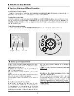
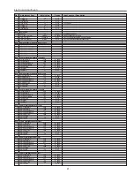
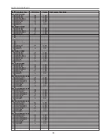
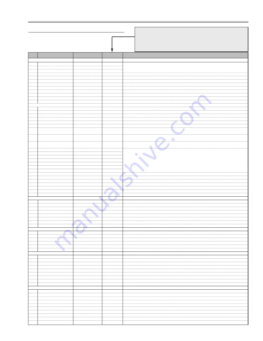
Service Adjustment Data Table
These initial values are the reference data written from the CPU
ROM to memory IC when replaced new memory IC. The adjust-
ment items indicated with “
✻
” are required to readjust following
to the “Electrical adjustments”. Other items should be used with
the initial data value.
Group: 0 AD9882
0
ADC G-OFFSET
81/103/72
0 ~ 127
✻
Clamp Adjustment [G]
1
ADC R-OFFSET
69/79/78
0 ~ 127
PC/AV30KHz/AV15KHz
✻
Clamp Adjustment [R]
2
ADC B-OFFSET
76/82/81
0 ~ 127
✻
Clamp Adjustment [B]
3
ADC R-GAIN
78/78/78
0 ~ 255
PC/AV30KHz/AV15KHz
4
ADC G-GAIN
78/78/78
0 ~ 255
PC/AV30KHz/AV15KHz
5
ADC B-GAIN
78/78/78
0 ~ 255
PC/AV30KHz/AV15KHz
6
ADC BandWidth PC
1
0 ~ 1
7
ADC BandWidth AV
0
0 ~ 1
8
ADC BandWidth DVI
1
0 ~ 1
9
ADC BandWidth HDCP
1
0 ~ 1
10
ADC BandWidth YCbCr
0
0 ~ 1
Only 1080i/1035i/720p, others are contained in AV
Group: 2 TB1274
0
Y_OUT_LEVEL_CONTROL
0
-63 ~ 63
(YCbCr 480i)
1
C_OUT_LEVEL_CONTROL
0
-63 ~ 63
(YCbCr 480i)
2
TINT
30/32
0 ~63
CVBS/YC
3
SHP_EQ
2
0 ~ 3
4
SHP_FO
2
0 ~ 3
5
SHP_GAIN
12/10/10/10/10/8/11/11
0 ~15
VideoNT/ PAL,PALM,PALN/SECAM,BW60,BW50/ NT443/ PAL60/ S-Video/YCbCr/Scart
6
Y_OUT_LEVEL
24/24/24/24/28
0 ~ 63
VideoNT/ NT443/ PAL,PALM,PALN/ PAL60/ SECAM,BW
0.7V
24/24/24/24/24/27/24
S-VideoNT,BW/ NT443/ PAL,PALM,PALN/ PAL60/ SECAM/ YCbCr/Scart
7
C_OUT_LEVEL
12/13/15/13/22
0 ~ 63
VideoNT/ NT443/ PAL,PALM,PALN/ PAL60/ SECAM,BW
0.6V
12/13/15/13/22/17/17/21
S-VideoNT,BW/ NT443/ PAL,PALM,PALN/ PAL60/ SECAM/480i/575i/Scart
8
Y_DELAY
5/5/4/4/4
0 ~ 15
Video NT,BW60/ PAL,PALM,PALN,BW50/ SECAM/NT443/PAL60
4/4/3/3/4
S-Video NT,BW60/PAL,PALM,PALN,BW50/ SECAM/ NT443/ PAL60
9
COL_SYS
-
-
Read Only
10
X'TAL
-
-
11
NOISE_DET
-
-
12
V_FREQ
-
-
13
Vert. Std
-
-
14
CID
-
-
15
V_SIG
-
-
16
MVM
0
0 or 1
17
AFC_GAIN
1
0 ~ 3
18
SECAM_GP,SECAM_ID
7
0 ~ 15
19
LPF
1/1
0 or 1
Scart/not Scart
20
Cb OFFSET1
8
0-15
21
Cr OFFSET1
8
0-15
Group: 3 TA1370
0
SEP.LEVEL
1
0 ~ 3
1
HD1 OUT SET
1
0 ~ 1
2
HD PHASE
29/29/36/38/36
0 ~ 63
1080i/1035i/720p/575p/480p
3
VD1 INV
0
0 ~ 1
4
V-FREQ
0 ~ 127
read only
5
HD-IN
0 ~ 1
read only
6
H-FREQ
0 ~ 127
read only
Group: 7 TC90A69F
0
Y-EQ_GAIN
3
0 ~ 3
1
Y-EQ_N_C_LIM
1
0 ~ 3
2
V-ENH_GAIN
1
0 ~ 7
3
V_ENH_CORING
2
0 ~ 3
4
NTSC443_SW
1
0 ~ 1
Set for Input system 0:NTSC4.431:PAL60(Effective only NTSC input)
Group: 8 LP05
0
LP05_R_GAIN_ud
128
0 ~ 255
Turbo R Gain (128 at through)
1
LP05_G_GAIN_ud
128
0 ~ 255
Turbo G Gain (128 at through)
2
LP05_B_GAIN_ud
128
0 ~ 255
Turbo B Gain (128 at through)
3
LP05_TURBO_GAIN_ud
0
0 ~ 255
Turbo mixture ratio (0 at through)
4
LP05_SHP_EN_SET_ud
162/262
0 ~ 4095
Set Aperture Compensation effective period SVGA/XGA
5
LP05_SHP_EN_RST_ud
958/1281
0 ~ 4095
Set Aperture Compensation effective period SVGA/XGA
6
LP05_AB_ON_ud
3
0 ~ 3
Set Aperture Comp. period selection (points) 3: 3, 1: 2, 0: 1, 2: not selectable
7
LP05_EGE_ud
2
0 ~ 3
Selection Data for Frequency Characteristics
Group: 9 CXD3536R (Panel Drive System)
0
DCK_CDAT
Read Only
[Addr:0x1043]
1
G_SUB_GAIN
71/70/61/61
0 ~ 255
[Addr:0x2007] PC/AV/DVI/HDCP
✻
Sub Gain Adjustment [G]
2
R_SUB_GAIN
71/70/61/61
0 ~ 255
[Addr:0x2006] PC/AV/DVI/HDCP
✻
Sub Gain Adjustment [R]
3
B_SUB_GAIN
71/70/61/61
0 ~ 255
[Addr:0x2008] PC/AV/DVI/HDCP
✻
Sub Gain Adjustment [B]
4
G_SUB_BRT
0
0 ~ 2047
[Addr:0x200B-200C] Signed 11bit
5
R_SUB_BRT
0
0 ~ 2047
[Addr:0x2009-200A] Signed 11bit
6
B_SUB_BRT
0
0 ~ 2047
[Addr:0x200D-200E] Signed 11bit
7
G_GAM_GAIN
128
0 ~ 255
[Addr:0x202C]
8
R_GAM_GAIN
128
0 ~ 255
[Addr:0x202B]
9
B_GAM_GAIN
128
0 ~ 255
[Addr:0x202D]
No.
Adjustment Item
Initial Value
Range
Input source / Description
Summary of Contents for PLC-XU50
Page 51: ... 51 IC Block Diagrams AD8075 Selector IC201 AN7513 Audio Output IC5601 ...
Page 52: ... 52 BA7078 Sync Separator IC5341 IC Block Diagrams AN5870 RGB SYNC SW IC1201 IC5201 ...
Page 54: ... 54 FA5502 P F Control IC621 IC Block Diagrams CXD3536 LCD Driver IC401 ...
Page 55: ... 55 IC Block Diagrams M62392 M62393 D A IC6271 IC281 ML60851 USB Driver IC9801 ...
Page 56: ... 56 STR Z2156 Power Switching Control IC631 TB1274 Video Decoder IC3101 IC Block Diagrams ...
Page 57: ... 57 IC Block Diagrams TC90A69F Y C Separator IC2101 ...
Page 86: ...MW3 XU5000 MT3 XU5500 86 S5 S5 S5 L9 Projection Mechanical Parts List ...
Page 89: ...MW3 XU5000 MT3 XU5500 89 ...
Page 90: ... MT3A Sep 2003 BB 400 Printed in Japan SANYO Electric Co Ltd ...

