


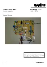

Service manual
CHASSIS 2112-Series EC7-A
1
INDEX
1.
SAFETY INSTRUCTIONS..................................................................................................................................... 3
1.1
W
ARNING
. ........................................................................................................................................................ 3
1.2
P
RECAUTIONS AGAINST
X-R
AYS
. ....................................................................................................................... 3
1.3
R
ECOMMENDATIONS TO PROTECT OUR ENVIRONMENT
......................................................................................... 3
1.4
S
AFETY AND
EMC (E
LECTROMAGNETIC
C
OMPATIBILITY
). ................................................................................... 3
2.
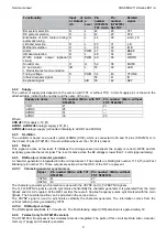
TECHNICAL CHARATERISTICS. ........................................................................................................................ 4
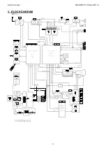
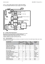
3.
BLOCK DIAGRAM ................................................................................................................................................ 5
3.1
I
NTEGRATED CIRCUITS
. ...................................................................................................................................... 6
4.
DETAILED DESCRIPTION IN BLOCKS .............................................................................................................. 6
4.1
P
OWER SUPPLY
. ............................................................................................................................................... 6
4.1.1
Switched Mode Power Supply (SMPS)..................................................................................................... 6
4.1.1.1
IC800 controller start-up..................................................................................................................... 6
4.1.2
Normal functioning ("on"). ......................................................................................................................... 6
4.1.2.1
Duty cycle. .......................................................................................................................................... 6
4.1.2.2
Regulation. ......................................................................................................................................... 6
4.1.3
"Stand-by". ................................................................................................................................................ 7
4.1.4
“+8v” and “+5v” regulators ........................................................................................................................ 7
4.1.4.1
Configuration. ..................................................................................................................................... 7
4.1.4.2
“stand-by” / ”ON” control .................................................................................................................... 7
4.1.4.3
Regulator output short circuit protection. ........................................................................................... 7
4.1.4.4
Mains switch off detection. ................................................................................................................. 7
4.1.4.5
Power supply signals and micro signals interrelation......................................................................... 8
4.2
T
ELETEXT AND MICROPROCESSOR
. .................................................................................................................... 8
4.2.1
Ports description. ...................................................................................................................................... 8
4.2.2
Supply. ...................................................................................................................................................... 9
4.2.3
Oscillator................................................................................................................................................... 9
4.2.4
Reset. ....................................................................................................................................................... 9
4.2.5
RGB output, character generator.............................................................................................................. 9
4.2.5.1
Character generator synchronism...................................................................................................... 9
4.2.5.2
RGB output voltage. ........................................................................................................................... 9
4.2.6
Teletext (only for ST92195 version).......................................................................................................... 9
4.2.6.1
Non-interlaced. ................................................................................................................................. 10
4.2.7
–PD signal. ............................................................................................................................................. 10
4.2.8
ON signal. ............................................................................................................................................... 10
4.2.9
Radio control signals. ............................................................................................................................. 10
4.2.10
SC signal. ............................................................................................................................................ 10
4.2.11
–SUP_FAIL signal. .............................................................................................................................. 10
4.2.12
–AM/SCART signal.............................................................................................................................. 10
4.2.13
–LP/L signal......................................................................................................................................... 10
4.2.14
–AM/FM signal..................................................................................................................................... 10
4.2.15
–DEFL_FAIL signal. ............................................................................................................................ 10
4.2.16
I2C bus and peripherics connected to (SDA y SCL). .......................................................................... 10
4.2.17
CF1 and CF2 signals........................................................................................................................... 10
4.2.18
Tuning control signals (-AGC_LS, -LB, -MB, -HB, VTUNE). ............................................................... 10
4.2.19
BEEP signal......................................................................................................................................... 11
4.2.20
WIDTH signal. ..................................................................................................................................... 11
4.2.21
MUTE signal. ....................................................................................................................................... 11
4.2.22
LED signal. .......................................................................................................................................... 11
4.2.23
Customer instructions reception (IR and KEY signals). ...................................................................... 11
4.3
H
ORIZONTAL DEFLECTION
. ............................................................................................................................... 11
4.3.1
Driver stage. ........................................................................................................................................... 11
4.3.1.1
Driver stage power. .......................................................................................................................... 11
4.3.1.2
Driver stage start-up......................................................................................................................... 11
4.3.2
Line stage. .............................................................................................................................................. 11
4.3.3
Width adjustment. ................................................................................................................................... 12
4.3.4
H_FLY&SYNC signal generation. ........................................................................................................... 12
4.3.5
Recovered line voltages. ........................................................................................................................ 12
Summary of Contents for CE14A2-C
Page 20: ...Service manual CHASSIS 2112 Series EC7 A 5 3 BLOCK DIAGRAM ...
Page 48: ......


