Operations & Installation
2-24
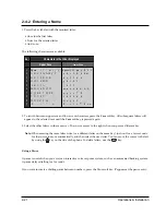
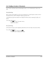
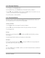
2-4-5 Erasing All Numbers
1. Press the
Menu
soft key.
Phonebook
appears.
2. Press the
Select
soft key to access
Phonebook
menu. The phonebook options are displayed.
3. Press the
soft key until
All Erase
is selected, then press the
Select
soft key. You are asked if you are sure
you want to erase all numbers stored in your phonebook memory.
4. Press the
Yes
soft key to confirm the deletion.
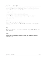
2-4-6 Phonebook Options
When you are viewing a number in the Phonebook,
Options
appears above the left soft key to allow you to
access the phonebook options, described in the following paragraphs.
Accessing to the Options
1. Press the
Options
soft key when it appears. The options are displayed.
2. Press the
soft key until a desired option is selected. The option in bold type will be selected.
3. Press the
Select
soft key.
Edit Name
Edit the name by using the keypad and the
key, then press the
OK
soft key. For details on entering a
name, see page 33.
Your phone displays the newly edited name, its number and its address number.
Edit Number
Edit the number by using the keypad and the
key, then press the
OK
soft key. Your phone displays the
newly edited number, its name and its address number.
Erase
If you press the
Select
soft key when
Erase
is selected, you are asked to confirm the deletion. Press the
Yes
soft
key to confirm the deletion.
C
C
Summary of Contents for SP-R6100
Page 3: ......
Page 52: ...Exploded View Parts List 3 6 3 6 SP R6100 CHARGER Exploded View 6 8 7 1 2 3 4 5 9 ...
Page 54: ...Exploded View Parts List 3 8 SP R6100 PACKING Exploded View 3 8 3 7 4 1 5 8 2 6 9 ...
Page 67: ...6 1 6 PCB Diagrams 6 1 SP R6100 Base PCB I ...
Page 68: ...PCD Diagrams ...
Page 69: ...6 2 SP R6100 Base PCB II 6 2 ...
Page 70: ...PCD Diagrams ...
Page 71: ...6 3 SP R6100 Handy PCB I 6 3 ...
Page 72: ...PCD Diagrams ...
Page 73: ...6 4 SP R6100 Handy PCB II 6 4 ...
Page 74: ...PCD Diagrams ...
Page 75: ...6 5 SP R6100 Key PCB I PCD Diagrams 6 5 ...
Page 76: ...6 6 SP R6100 Key PCB II PCB Diagrams 6 6 ...
Page 77: ...6 7 SP R6100 Charger PCB I 6 7 PCD Diagrams ...
Page 78: ...6 8 SP R6100 Charger PCB II PCB Diagrams 6 8 ...
Page 79: ...Schematic Diagrams 7 1 7 Schematic Diagrams 7 1 SP R6100 Hand LOGIC ...
Page 81: ...Schematic Diagrams 7 3 7 3 SP R6100 BASE LOGIC ...
Page 82: ...Schematic Diagrams 7 4 7 4 SP R6100 Base CLIP ...
Page 84: ...Schematic Diagrams 7 6 HAND KEY 7 6 ...


