background image

S3F84B8_UM_REV 1.00 

21 ELECTRICAL DATA 

 21-7 


10 MHz

External Clock 

Frequency

8 MHz

1 MHz

1

1.8

4

5

6

7

Supply Voltage (V)

2 MHz

3 MHz

4 MHz

..

5.5

4.5

2.7

400KHz

2.0


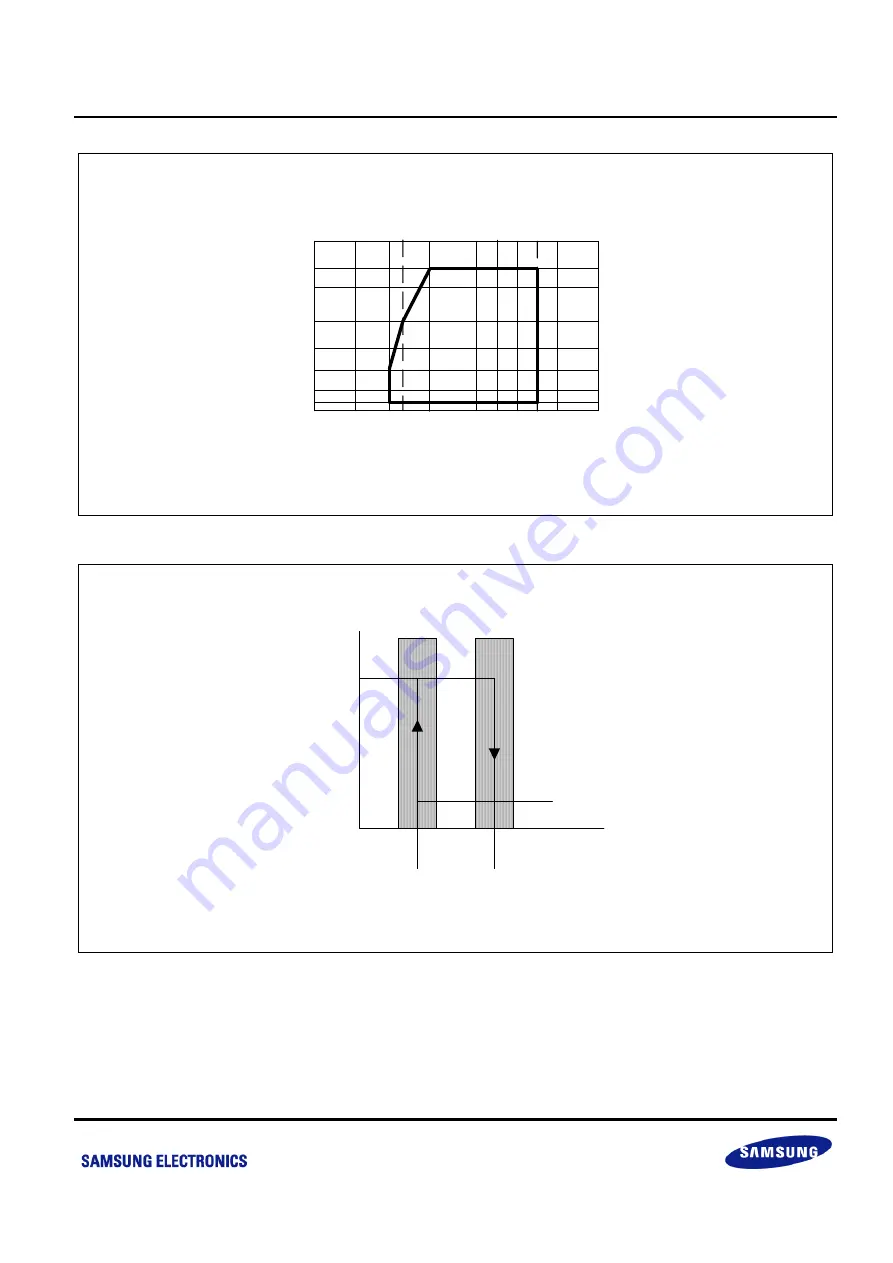
Figure 21-2      Operating Voltage Range @ External clock 

V

SS

A

A = 0.2 V

DD

B = 0.4 V

DD

C = 0.6 V

DD

D = 0.8 V

DD

V

DD

V

OUT

V

IN

B

C

D

0.3 V

DD

0.7 V

DD


Figure 21-3      Schmitt Trigger Input Characteristics Diagram 


Summary of Contents for S3F84B8

Page 1: ...S3F84B8 8 bit CMOS Microcontrollers Revision 1 00 June 2010 U Us se er r s s M Ma an nu ua al l 2010 Samsung Electronics Co Ltd All rights reserved ...

Page 2: ...technical experts Samsung products are not designed intended or authorized for use as components in systems intended for surgical implant into the body for other applications intended to support or sustain life or for any other application in which the failure of the Samsung product could create a situation where personal injury or death may occur Should the Buyer purchase or use a Samsung product...

Page 3: ...Revision History Revision No Date Description Author s 0 00 Sep 9 2009 Initial draft Wei Ningning 1 00 April 30 2010 Released version Wei Ningning ...

Page 4: ...ster Area C0H CFH 2 14 2 4 2 4 Bit Working Register Addressing 2 15 2 4 3 8 Bit Working Register Addressing 2 17 2 4 4 System and User Stack 2 19 2 4 4 1 Stack Operations 2 19 2 4 4 2 User defined Stacks 2 19 2 4 4 3 Stack Pointers SPL SPH 2 19 3 ADDRESSING MODES 3 1 3 1 Overview of Addressing Modes 3 1 3 2 Register R Addressing Mode 3 2 3 3 Indirect Register IR Addressing Mode 3 3 3 4 Indirect Re...

Page 5: ...P AMP Control Register E0H BANK1 4 21 4 1 22 P0CONH Port 0 Control Register High Byte E4H Bank0 4 22 4 1 23 P0CONL Port 0 Control Register Low Byte E5H BANK0 4 23 4 1 24 P0INT Port 0 Interrupt Control Register E3H BANK0 4 24 4 1 25 P0PND Port 0 Interrupt Pending Register E6H BANK0 4 25 4 1 26 P1CON Port 1 Control Register E7H BANK0 4 26 4 1 27 P2CONH Port 2 Control Register High Byte E8H BANK0 4 2...

Page 6: ...ruction Pointer IP 5 16 5 1 19 Fast Interrupt Processing 5 16 5 1 20 Procedure for Initiating Fast Interrupts 5 17 5 1 21 Fast Interrupt Service Routine 5 17 5 1 22 Relationship to Interrupt Pending Bit Types 5 17 5 1 23 Programming Guidelines 5 17 6 INSTRUCTION SET 6 1 6 1 Overview of Instruction Set 6 1 6 1 1 Key Features of Instruction Set 6 1 6 1 1 1 Data Types 6 1 6 1 1 2 Register Addressing ...

Page 7: ...Load Memory and Increment 6 54 6 3 42 LDCPD LDEPD Load Memory with Pre Decrement 6 55 6 3 43 LDCPI LDEPI Load Memory with Pre Increment 6 56 6 3 44 LDW Load Word 6 57 6 3 45 MULT Multiply Unsigned 6 58 6 3 46 NEXT Next 6 59 6 3 47 NOP No Operation 6 60 6 3 48 OR Logical OR 6 61 6 3 49 POP Pop From Stack 6 62 6 3 50 POPUD Pop User Stack Decrementing 6 63 6 3 51 POPUI Pop User Stack Incrementing 6 6...

Page 8: ...rt Data Registers 9 1 9 1 1 1 Port 0 9 2 9 1 1 2 Port 1 9 7 9 1 1 3 Port 2 9 9 10 BASIC TIMER 10 1 10 1 Overview of Basic Timer 10 1 10 2 Basic Timer Control Register BTCON 10 2 10 2 1 Basic Timer Function Description 10 3 10 2 1 1 Watchdog Timer Function 10 3 10 2 1 2 Oscillation Stabilization Interval Timer Function 10 3 11 8 BIT TIMER A 11 1 11 1 Overview of 8 bit Timer A 11 1 11 1 1 Functional...

Page 9: ... Comparator 14 1 14 1 1 Functional Description of Comparator 14 1 14 1 1 1 Comparator 0 14 1 14 1 1 2 Comparator 1 2 3 14 4 15 OPERATIONAL AMPLIFIER 15 1 15 1 Overview of Operational Amplifier 15 1 15 1 1 Functional Description of Operational Amplifier 15 1 15 1 2 OPAMP Control Register 15 2 15 1 3 Block Diagram of OPAMP 15 2 15 1 4 Reference Circuit 15 3 16 10 BIT IH PWM 16 1 16 1 Overview of 10 ...

Page 10: ...5 3 Flash Memory Sector Address Registers 19 4 19 1 6 Sector Erase 19 5 19 1 7 Programming 19 8 19 1 8 Reading 19 14 19 1 9 Hard Lock Protection 19 15 20 LOW VOLTAGE RESET 20 1 20 1 Overview of Low Voltage Reset 20 1 21 ELECTRICAL DATA 21 1 21 1 Overview of Electrical Data 21 1 22 DEVELOPMENT TOOLS 22 1 22 1 Overview of Development Tools 22 1 22 1 1 Target Boards 22 1 22 1 2 Programming Socket Ada...

Page 11: ...gister File Addressing 2 13 Figure 2 11 Common Working Register Area 2 14 Figure 2 12 4 Bit Working Register Addressing 2 15 Figure 2 13 4 Bit Working Register Addressing Example 2 16 Figure 2 14 8 Bit Working Register Addressing 2 17 Figure 2 15 8 Bit Working Register Addressing Example 2 18 Figure 2 16 Stack Operations 2 19 Figure 3 1 Register Addressing 3 2 Figure 3 2 Working Register Addressin...

Page 12: ...ET 8 3 Figure 9 1 Port 0 Control Register High Byte P0CONH 9 3 Figure 9 2 Port 0 Control Register Low Byte P0CONL 9 4 Figure 9 3 Port 0 Interrupt Control Register P0INT 9 5 Figure 9 4 Port 0 Interrupt Pending Register P0PND 9 6 Figure 9 5 Port 1 Control Register P1CON 9 8 Figure 9 6 Port 2 High Byte Control Register P2CONH 9 10 Figure 9 7 Port 2 Low Byte Control Register P2CONL 9 11 Figure 10 1 Ba...

Page 13: ... of PWM and Comparator 0_Delay Trigger 16 7 Figure 16 7 Example of the cooperation of PWM and Comparator 0_Anti mis Trigger 16 7 Figure 16 8 Example of the Cooperation of PWM and Comparator 1 2 3_ Hard Lock 16 8 Figure 16 9 Example of the Cooperation of PWM and Comparator 1 2 3_Soft Lock 16 8 Figure 17 1 Buzzer Control Register BUZCON 17 1 Figure 17 2 BUZ Functional Block Diagram 17 3 Figure 18 1 ...

Page 14: ...rget Board Configuration 22 3 Figure 22 3 DIP Switch for Smart Option 22 6 Figure 22 4 40 Pin Connector for TB84B8 22 7 Figure 22 5 S3F84B8 Probe Adapter for 20 DIP Package 22 7 Figure 23 1 20 DIP 300A Package Dimensions 23 1 Figure 23 2 20 SOP 375 Package Dimensions 23 2 ...

Page 15: ...after RESET 8 6 Table 8 2 System and Peripheral Control Registers Set1 Bank1 8 8 Table 9 1 S3F84B8 Port Configuration Overview 9 1 Table 9 2 Port Data Register Summary 9 1 Table 16 1 PWM Control and Data Registers 16 2 Table 17 1 Buzzer Frequency Table 4MHz 17 2 Table 18 1 Descriptions of Pins Used to Read Write the Flash ROM 18 2 Table 21 1 Absolute Maximum Ratings 21 2 Table 21 2 DC Electrical C...

Page 16: ...Table 22 1 TB84B8 Components 22 4 Table 22 2 Power Selection Settings for TB84B8 22 4 Table 22 3 Using Single Header Pins to Select Clock Source and Enable Disable PWM 22 5 ...

Page 17: ...ple 2 3 Addressing the Common Working Register Area 2 14 Example 2 4 Standard Stack Operations Using PUSH and POP 2 20 Example 10 1 Configuring the Basic Timer 10 6 Example 13 1 Configuring A D Converter 13 6 Example 14 1 Comparator Configuration 14 7 Example 19 1 Sector Erase 19 7 Example 19 2 Programming 19 11 Example 19 3 Reading 19 14 Example 19 4 Hard Lock Protection 19 15 ...

Page 18: ...B8 specifies a microcontroller with built in 8K byte full flash ROM Using a proven modular design approach Samsung S3F84B8 integrates the following peripheral modules with a powerful SAM8 RC core 3 configurable I O ports 18 pins 17 interrupt sources with 17 vectors and 6 interrupt levels 1 watchdog timer function Basic Timer 1 basic timer 8 bit for oscillation stabilization 3 timer counters 8 bit ...

Page 19: ...erase 32ms o Sector erase 12ms o Byte program 20us User programmable by LDC instruction Endurance 10 000 erase program cycles Sector 128 bytes erase available Byte programmable 272 byte general purpose register area Instruction Set 78 instructions Idle and Stop instructions added for power down modes Instruction Execution Time 400ns at 10MHz fOSC minimum Interrupts 17 Interrupt sources with 17 vec...

Page 20: ...tion OP Amplifier 1 integrated OP Amplifier Timer Counters 1 basic timer 8 bit for watchdog function 1 timer 8 bit TimerA Interval mode Capture mode 8 bit PWM mode 1 timer counter 16 bit Timer0 Configurable to 2 timer counters 8 bit Interval mode CMP0 event counter mode 6 7 8 bit PWM mode BUZ 1 programmable Buzzer Oscillation Frequency 1MHz to 10MHz external crystal oscillator Typical 8MHz externa...

Page 21: ...t in RESET Circuit LVR Low voltage check to reset system VLVR 1 9 2 3 3 0 3 6 3 9V by smart option Operating Temperature Range 40 C to 85 C Operating Voltage Range 1 8V to 5 5V 0 4 2MHz 2 0V to 5 5V 0 4 4MHz 2 7V to 5 5V 0 4 10M Hz Package Types S3F84B8 20 SOP 20 DIP ...

Page 22: ...errupt Control SAM8 RC CPU 8 Kbyte ROM 272 Byte RAM OSC nRESET 8 Bit Basic Timer 8 Bit Timer Counter A A D Port 0 P0 0 0 6 INT0 INT5 P2 0 2 7 P1 0 1 2 XIN XOUT P0 2 nRESET TAOUT TACK ADC0 7 Port 2 Port 1 BUZ TACAP CMP3 CMP0 CMP1 CMP2 8 Bit Timer C D BUZ TDOUT OPAMP PWM CMP0_N PWM CMP0_P CMP1_N CMP2_N CMP3_N OA_O OA_P OA_N Figure 1 1 S3F84B8 Block Diagram ...

Page 23: ...9 18 17 16 15 14 13 12 11 1 2 3 4 5 6 7 8 9 10 VDD P2 7 ADC7 SCL P2 6 ADC6 SDA P2 5 ADC5 CMP3_N P2 4 ADC4 CMP2_N P2 3 ADC3 OPA_O P2 2 ADC2 OPA_N P2 1 ADC1 OPA_P P2 0 ADC0 TDOUT P1 2 CMP1_N VSS INT0 XIN P0 0 INT1 XOUT P0 1 VPP nRESET P0 2 BUZ INT2 P0 3 PWM INT3 P0 4 INT4 P0 5 TAOUT INT5 P0 6 TACK CMP0_P P1 0 ACAP CMP0_N P1 1 Figure 1 2 S3F84B8 Pin Assignment 20 DIP 20 SOP ...

Page 24: ...put or Timer counter A PWM output 1 3 8 P0 6 TACK I Timer counter A external clock input 1 1 9 P1 0 TACAP I Timer counter A external capture input 1 1 10 P1 1 TDOUT O Timer counter D match output or Timer counter D PWM output 1 1 12 P2 0 CMP0_P I Comparater0 positive input pin 1 1 9 P1 0 CMP0_N I Comparater0 negative input pin 1 1 10 P1 1 CMP1_N I Comparater1 negative input pin 1 1 11 P1 2 CMP2_N ...

Page 25: ...in No I O Function P2 6 SDA 18 I O Serial data pin output when reading Input when writing Input and push pull output port can be assigned P2 7 SCL 19 I Serial clock pin input only pin RESET P0 2 VPP 4 I Power supply pin for flash ROM cell writing indicates that MTP enters into the writing mode When 11 V is applied MTP is in the writing mode and when 5 V is applied MTP is in the reading mode Option...

Page 26: ...ITS Figure 1 3 shows the pin circuit type 1 in S3F84B8 P Channel N Channel VDD Out Output Disable Data Figure 1 3 Pin Circuit Type 1 Figure 1 4 shows the pin circuit type 2 in S3F84B8 P Channel N Channel VDD Out Output Disable Data Open drain enable Figure 1 4 Pin Circuit Type 2 ...

Page 27: ...10 Figure 1 5 shows the pin circuit type 1 1 P1 0 1 2 P2 0 2 2 P2 4 2 7 in S3F84B8 VDD I O Digital Input Pull up enable Output Disable Input Mode Data Analog Input Enable Analog Input Pin Circuit Type 1 Figure 1 5 Pin Circuit Type 1 1 P1 0 1 2 P2 0 2 2 P2 4 2 7 ...

Page 28: ...CONTROLLER 1 11 Figure 1 6 shows the Pin Circuit Type 1 2 P2 3 in S3F84B8 VDD I O Digital Input Pull up enable Output Disable Input Mode Data Analog Input Enable Analog Input Pin Type 1 OPA output OPA Enable Bit Figure 1 6 Pin Circuit Type 1 2 P2 3 ...

Page 29: ...Pull up register 50 kohm typical Noise Filter Ext INT Input MUX Pin config bits Figure 1 7 Pin Circuit Type 1 3 P0 3 P0 4 P0 6 Figure 1 8 shows the Pin Circuit Type 2 1 P0 5 in S3F84B8 VDD I O Output DIsable input mode Data Pull up register 50 kohm typical Pull up enable Pin Circuit Type 2 Open drain enable Noise Filter Ext INT MUX Pin configure bits Input Figure 1 8 Pin Circuit Type 2 1 P0 5 ...

Page 30: ...Pin Circuit Type 3 P0 2 Figure 1 10 shows the Pin Circuit Type 2 2 P0 0 P0 1 in S3F84B8 VDD I O Output Disable input mode Data Xin Pull up enable MUX Smart option Pin Circuit Type 2 MUX Pull up register 50 kohm typical MUX Xout Open drain enable Noise Filter Ext INT MUX Pin config bits input Figure 1 10 Pin Circuit Type 2 2 P0 0 P0 1 ...

Page 31: ... 16 bit address bus supports program memory operations On the other hand a separate 8 bit register bus carries addresses and data between the CPU and internal register file The S3F84B8 microcontroller contains 8Kbytes of on chip program memory configured as Internal ROM It also contains 272 general purpose registers in the internal register file where 59 bytes are mapped for system and peripheral ...

Page 32: ...s Unused locations except 3CH 3DH 3EH 3FH in this address range can be used as normal program memory If you use the vector address area to store a program code do not overwrite the vector addresses stored in these locations 003CH 003DH 003EH and 003FH are used as smart option ROM cells The default program reset address in the ROM is 0100H 0100H Interrupt Vector Area 003FH 003CH 0000H Decimal HEX 0...

Page 33: ...110 2 3 V 100 3 0 V 001 3 6V 011 3 9 V ROM Address 003FH 7 6 5 4 3 2 1 0 MSB LSB Not used P0 2 nRESET pin selection bit 0 P0 2 pin enable 1 nRESET Pin enable Oscillation selection bit 00 External crystal Xin Xtout pin enable 01 External RC Xin Xtout pin enable 10 Internal oscillator 0 5MHz P0 0 P0 1 are normal IOs 11 Internal oscilator 8MHz P0 0 P0 1 are normal IOs ROM Address 003CH 7 6 5 4 3 2 1 ...

Page 34: ...heral control and data registers 16 bytes are meant for shared working registers 272 registers are meant for general purpose use page 0 For more information about page 0 refer to Figure 2 3 Registers in Set 1 can only be addressed using register addressing modes The extension of register space into separately addressable areas sets banks and pages is supported by various addressing mode restrictio...

Page 35: ...Registers Bank 0 System and Peripheral Control Registers Register Addressing Mode Set1 FFH E0H 32 Bytes E0H DFH D0H CFH C0H Page 0 Prime Data Registers All Addressing Modes Page 0 Set 2 General Purpose Data Registers Indirect Register Indexed Mode and Stack Operations C0H BFH 00H FFH 192 Bytes 64 Bytes 256 Bytes Figure 2 3 Internal Register File Organization in S3F84B8 ...

Page 36: ...alue lower nibble and the destination value upper nibble are always 0000 automatically selecting page 0 as the source and destination page for register addressing Register Page Pointer PP DFH Set 1 R W LSB MSB 7 6 5 4 3 2 1 0 Destination register page selection bits NOTE A hardware reset operation writes the 4 bit destination and source values shown above to the register page pointer These values ...

Page 37: ...e register file Using the Register Addressing mode the registers in set 1 location can be directly accessed at any time The 16 byte working register area can only be accessed using working register addressing For more information about working register addressing refer to Chapter 3 Addressing Modes 2 3 1 2 Register Set 2 The same 64 byte physical space that is used for set 1 location C0H FFH is lo...

Page 38: ...The prime register area on page 0 the prime register area on page 0 can be addressed immediately after a reset But to address prime registers on page 0 or 1 you must set the register page pointer PP to its appropriate source and destination values FFH FCH E0H D0H C0H Set 1 Bank 0 Peripheral and I O General purpose CPU and system control LCD data register FFH Page 1 Set 2 FFH C0H 00H BFH Page 0 Set...

Page 39: ...ions of selected working register spaces One working register slice is 8 bytes eight 8 bit working registers R0 R7 or R8 R15 One working register block is 16 bytes sixteen 8 bit working registers R0 R15 All the registers in an 8 byte working register slice have the same binary value for their five most significant address bits This makes it possible for each register pointer to point to one of the...

Page 40: ...g modes Usually the selected 16 byte working register block consists of two contiguous 8 byte slices As a general programming guideline it is recommended that RP0 point to the lower slice and RP1 point to the upper slice see Figure 2 7 In some cases it may be necessary to define working register areas in different non contiguous areas of the register file In Figure 2 7 RP0 and RP1 point to the upp...

Page 41: ... R1 R0 R0 R1 ADC R0 R2 R0 R0 R2 C ADC R0 R3 R0 R0 R3 C ADC R0 R4 R0 R0 R4 C ADC R0 R5 R0 R0 R5 C The sum of these six registers 6FH is located in the register R0 80H The instruction string used in this example takes 12 bytes of instruction code and its execution time is 36 cycles If the register pointer is not used to calculate the sum of these registers the following instruction sequence should b...

Page 42: ...ter file and an 8 bit register within that space Registers are addressed either as a single 8 bit register or a paired 16 bit register space In a 16 bit register pair the address of first 8 bit register is always an even number and the address of next register is always an odd number The most significant byte MSB of 16 bit data is always stored in the even numbered register and the least significa...

Page 43: ...egisters Special Purpose Registers D0H C0H Bank 1 Bank 0 NOTE In the S3F84B8 microcontroller page 0 1 are implemented Each register pointer RP can independently point to one of the 24 8 byte slices of the register file other than set 2 After a reset RP0 points to locations C0H C7H and RP1 to locations C8H CFH that is to the common working register area FFH C0H Set 2 Prime Registers CFH General Pur...

Page 44: ...erent pages FFH Page 1 Set 2 FFH C0H 00H BFH Page 0 Set 2 Page 0 Prime Space FFH FCH E0H D0H C0H Set 1 Following a hardware reset register pointers RP0 and RP1 point to the common working register area locations C0H CFH RP0 RP1 1 1 0 0 0 0 0 0 1 1 0 0 1 0 0 0 Figure 2 11 Common Working Register Area Example 2 3 Addressing the Common Working Register Area As shown in the following examples you shou...

Page 45: ...t address select one of the eight registers in the slice As shown in Figure 2 12 the result of this operation is that the five high order bits from register pointer are concatenated with the three low order bits from instruction address to form the complete address If the address stored in register pointer remains unchanged the three bits from the address will always point to an address in the sam...

Page 46: ... 1 00 2 ADDRESS SPACES 2 16 Register address 76H RP0 0 1 1 1 0 0 0 0 0 1 1 1 0 1 1 0 R6 0 1 1 0 1 1 1 0 Selects RP0 Instruction INC R6 OPCODE RP1 0 1 1 1 1 0 0 0 Figure 2 13 4 Bit Working Register Addressing Example ...

Page 47: ... complete address are provided by the original instruction Figure 2 15 shows an example of 8 bit working register addressing The four high order bits of instruction address 1100B specify the 8 bit working register addressing Bit 4 1 selects RP1 and the five high order bits in RP1 10101B become the five high order bits of register address The three low order bits of register address 011 are provide...

Page 48: ... 8 bit address form instruction LD R11 R2 RP0 0 1 1 0 0 0 0 0 1 1 0 0 1 0 1 1 Selects RP1 R11 Register address 0ABH RP1 1 0 1 0 1 0 0 0 1 0 1 0 1 0 1 1 Specifies working register addressing Figure 2 15 8 Bit Working Register Addressing Example ...

Page 49: ...You can freely define stacks in the internal register file as data storage locations The instructions PUSHUI PUSHUD POPUI and POPUD support user defined stack operations 2 4 4 3 Stack Pointers SPL SPH Register locations D8H and D9H contain the 16 bit stack pointer SP that is used for system stack operations The most significant byte of the SP address SP15 SP8 is stored in the SPH register D8H and ...

Page 50: ...al register file using PUSH and POP instructions LD SPL 0FFH SPL FFH Normally the SPL is set to 0FFH by the initialization routine PUSH PP Stack address 0FEH PP PUSH RP0 Stack address 0FDH RP0 PUSH RP1 Stack address 0FCH RP1 PUSH R3 Stack address 0FBH R3 POP R3 R3 Stack address 0FBH POP RP1 RP1 Stack address 0FCH POP RP0 RP0 Stack address 0FDH POP PP PP Stack address 0FEH ...

Page 51: ...ed to determine the location of the data operand The operands specified in SAM8RC instructions can include condition codes immediate data or a location in the register file program memory or data memory The S3C series instruction set supports seven explicit addressing modes Not all of these addressing modes are available for each instruction The seven addressing modes and their symbols are Registe...

Page 52: ...ion OPCODE OPERAND 8 bit Register File Address Point to One Register in Register File One Operand Instruction Example Sample Instruction DEC CNTR Where CNTR is the label of an 8 bit register address Program Memory Register File Figure 3 1 Register Addressing dst OPCODE 4 bit Working Register Point to the Working Register 1 of 8 Two Operand Instruction Example Sample Instruction ADD R1 R2 Where R1 ...

Page 53: ... register to indirectly address another register Any 16 bit register pair can be used to indirectly address another memory location Note that you cannot access locations C0H FFH in set 1 using the Indirect Register addressing mode dst Address of Operand used by Instruction OPCODE ADDRESS 8 bit Register File Address Point to One Register in Register File One Operand Instruction Example Sample Instr...

Page 54: ...PCODE PAIR Points to Register Pair Example Instruction References Program Memory Sample Instructions CALL RR2 JP RR2 Program Memory Register File Value used in Instruction OPERAND REGISTER Program Memory 16 Bit Address Points to Program Memory Figure 3 4 Indirect Register Addressing to Program Memory ...

Page 55: ... Working Register Address Point to the Working Register 1 of 8 Sample Instruction OR R3 R6 Program Memory Register File src 3 LSBs Value used in Instruction OPERAND Selected RP points to start fo working register block RP0 or RP1 MSB Points to RP0 or RP1 Figure 3 5 Indirect Working Register Addressing to Register File ...

Page 56: ...ccess Program Memory Register File src Value used in Instruction OPERAND Example Instruction References either Program Memory or Data Memory Program Memory or Data Memory Next 2 bit Point to Working Register Pair 1 of 4 LSB Selects Register Pair 16 Bit address points to program memory or data memory RP0 or RP1 MSB Points to RP0 or RP1 Selected RP points to start of working register block Figure 3 ...

Page 57: ...is added to an 8 bit offset contained in a working register For external memory accesses the base address is stored in a working register pair designated in the instruction The 8 bit or 16 bit offset given in the instruction is then added to that base address see Figure 3 9 The only instruction that supports Indexed addressing mode for internal register file is the Load instruction LD The LDC and ...

Page 58: ... points to start of working register block Sample Instructions LDC R4 04H RR2 The values in the program address RR2 04H are loaded into register R4 LDE R4 04H RR2 Identical operation to LDC example except that external program memory is accessed NEXT 2 Bits Register Pair Value used in Instruction 8 Bits 16 Bits 16 Bits dst src OPCODE Program Memory x OFFSET 4 bit Working Register Address Figure 3 ...

Page 59: ...oints to start of working register block Sample Instructions LDC R4 1000H RR2 The values in the program address RR2 1000H are loaded into register R4 LDE R4 1000H RR2 Identical operation to LDC example except that external program memory is accessed NEXT 2 Bits Register Pair Value used in Instruction 8 Bits 16 Bits 16 Bits dst src OPCODE Program Memory src OFFSET 4 bit Working Register Address OFF...

Page 60: ...s mode to specify the source or destination address for Load operations to program memory LDC or external data memory LDE if implemented Sample Instructions LDC R5 1234H The values in the program address 1234H are loaded into register R5 LDE R5 1234H Identical operation to LDC example except that external program memory is accessed dst src OPCODE Program Memory 0 or 1 Lower Address Byte LSB Select...

Page 61: ...D OPCODE Program Memory Lower Address Byte Memory Address Used Upper Address Byte Sample Instructions JP C JOB1 Where JOB1 is a 16 bit immediate address CALL DISPLAY Where DISPLAY is a 16 bit immediate address Next OPCODE Figure 3 11 Direct Addressing for Call and Jump Instructions ...

Page 62: ...s mode Since the assumption in using Indirect Address mode is that the operand is located in the lowest 256 bytes of program memory only an 8 bit address is supplied in the instruction the upper bytes of destination address are assumed to be all zeros Current Instruction Program Memory Locations 0 255 Program Memory OPCODE dst Lower Address Byte Upper Address Byte Next Instruction LSB Must be Zero...

Page 63: ...tion occurs the PC contains the address of instruction immediately following the current instruction Several program control instructions use the Relative Address mode to perform conditional jumps The instructions that support RA addressing are BTJRF BTJRT DJNZ CPIJE CPIJNE and JR OPCODE Program Memory Displacement Program Memory Address Used Sample Instructions JR ULT OFFSET Where OFFSET is a val...

Page 64: ...s the value supplied in operand field itself The operand can be one byte or one word in length depending on the instruction used Immediate addressing mode is useful for loading constant values into registers The Operand value is in the instruction OPCODE Sample Instruction LD R0 0AAH Program Memory OPERAND Figure 3 14 Immediate Addressing ...

Page 65: ...0 Address and Location RESET Value Bit Register Name Mnemonic Address R W 7 6 5 4 3 2 1 0 Locations D0 D2H are not mapped Basic Timer Control Register BTCON D3H R W 0 0 0 0 0 0 0 0 Clock Control Register CLKCON D4H R W 0 0 0 System Flags Register FLAGS D5H R W x x x x x x 0 0 Register Pointer 0 RP0 D6H R W 1 1 0 0 0 Register Pointer 1 RP1 D7H R W 1 1 0 0 1 Location D8H is not mapped Stack Pointer ...

Page 66: ...MPINT EEH R W 1 1 1 1 1 1 1 1 PWM control register PWMCON EFH R W 0 0 0 0 0 0 0 0 PWM CMP register PWMCCON F0H R W 0 0 0 0 PWM delay trigger data register PWMDL F1H R W 0 0 0 0 0 0 0 0 PWM preset data register High byte PWMPDATAH F2H R W 0 0 0 0 0 0 0 0 PWM preset data register Low byte PWMPDATAL F3H R W 0 0 PWM data register High byte PWMDATAH F4H R W 0 0 0 0 0 0 0 0 PWM data register Low byte PW...

Page 67: ...er C counter register TCCNT E8H R x x x x x x x x Timer D control register TDCON E9H R W 0 0 0 0 0 0 0 0 Timer D clock pre scalar TDPS EAH R W 0 0 0 0 0 Timer D data register TDDATA EBH R W 1 1 1 1 1 1 1 1 Timer D counter register TDCNT ECH R x x x x x x x x Locations EDH F1H are not mapped Reset source indicating register RESETID F2H RW Refer to the detailed description Location F3H is not mapped...

Page 68: ...nded to the register name for bit addressing D5H Register address hexadecimal Register name Register ID Name of individual bit or related bits x R W x R W x R W x R W 0 R W x R W 0 R W x R W Carry Flag C 0 Operation dose not generate a carry or borrow condition 1 Operation generates carry out or borrow into high order bit7 Zero Flag 0 Operation result is a non zero value 1 Operation result is zero...

Page 69: ...5 1 1 0 ADC6 P2 6 7 5 1 1 1 ADC7 P2 7 AD Conversion Completion Interrupt Enable Bit 0 Disables ADC Interrupt 4 1 Enables ADC Interrupt A DC Interrupt Pending Bit EOC 0 No interrupt is pending conversion is in progress clears pending bit when write 3 1 Interrupt is pending conversion has completed no effect when write Clock Source Selection Bit Note 0 0 fOSC 8 fOSC 10MHz 0 1 fOSC 4 fOSC 10MHz 1 0 f...

Page 70: ...2 1 0 RESET Value 0 0 0 0 0 0 0 0 Read Write R W R W R W R W R W R W R W R W Watchdog Timer Function Enable Bit 1 0 1 0 Disables watchdog timer function 7 4 Others Enables watchdog timer function Basic Timer Input Clock Selection Code 0 0 fOSC 4096 0 1 fOSC 1024 1 0 fOSC 128 3 2 1 1 Invalid setting Basic Timer 8 Bit Counter Clear Bit 0 No effect 1 1 Clears the basic timer counter value Basic Timer...

Page 71: ...r 7 6 5 4 3 2 1 0 RESET Value 0 0 0 0 0 0 0 0 Read Write R W R W R W R W R W R W R W R W Addressing Mode Register addressing mode only BUZ Input Clock Selection Code 0 0 fOSC 16 0 1 fOSC 32 1 0 fOSC 64 7 6 1 1 fOSC 128 BUZ Enable Bit 0 Disables BUZ 5 1 Enables BUZ 4 0 BUZ Frequency fBUZ BUZCON 4 0 1 2 ...

Page 72: ...Oscillator IRQ Wake up Function Enable Bit 0 Enables IRQ for main system oscillator wake up function 7 1 Disables IRQ for main system oscillator wake up function 6 5 Not used for S3F84B8 Divided by Selection Bits for CPU Clock Frequency 0 0 Divide by 16 fOSC 16 0 1 Divide by 8 fOSC 8 1 0 Divide by 2 fOSC 2 4 3 1 1 Non divided clock fOSC 2 0 Not used for S3F84B8 ...

Page 73: ...s CMP0 output Comparator0 Enable Bit 2 0 Disables CMP0 3 1 Enables CMP0 Comparator0 Interrupt Enable Bit 0 Disables CMP0 interrupt 2 1 Enables CMP0 interrupt Comparator0 Status Bit 0 CMP0_N CMP0_P 1 1 CMP0_N CMP0_P Comparator0 Pending Bit 0 No interrupt is pending clears pending bit when write 0 1 CMP0 interrupt is pending NOTE 1 Polarity selection bit CMP0CON 4 will not affect the interrupt gener...

Page 74: ...mparator1 Output Polarity Select Bit 0 Does not invert CMP1 output 4 1 Inverts CMP1 output Comparator1 Enable Bit 0 Disables CMP1 3 1 Enables CMP1 Comparator1 Interrupt Enable Bit 0 Disables CMP1 interrupt 2 1 Enables CMP1 interrupt Comparator1 Status Bit 0 CMP1_N CMP1_P 1 1 CMP1_N CMP1_P Comparator1 Pending Bit 0 No interrupt is pending clears pending bit when write 0 1 CMP1 interrupt is pending ...

Page 75: ...mparator2 Output Polarity Select Bit 0 Does not invert CMP2 output 4 1 Inverts CMP2 output Comparator2 Enable Bit 0 Disables CMP1 3 1 Enables CMP1 Comparator2 Interrupt Enable Bit 0 Disables CMP1 interrupt 2 1 Enables CMP1 interrupt Comparator2 Status Bit 0 CMP2_N CMP2_P 1 1 CMP2_N CMP2_P Comparator2 Pending Bit 0 No interrupt is pending clears pending bit when write 0 1 CMP2 interrupt is pending ...

Page 76: ...3 Output Polarity Select Bit 0 Does not invert CMP3 output 4 1 Inverts CMP3 output Comparator3 Enable Bit 0 Disables comparator3 3 1 Enables comparator3 Comparator3 Interrupt Enable Bit 0 Disables CMP3 interrupt 2 1 Enables CMP3 interrupt Comparator3 Status Bit 0 CMP3_N CMP3_P 1 1 CMP3_N CMP3_P Comparator3 Pending Bit 0 No interrupt is pending clears pending bit when write 0 1 CMP3 interrupt is pe...

Page 77: ...CMP2 Interrupt mode selection bit 0 0 Invalid setting 0 1 Falling edge interrupt 1 0 Rising edge interrupt 5 4 1 1 Falling and rising edge interrupt CMP1 Interrupt mode selection bit 0 0 Invalid setting 0 1 Falling edge interrupt 1 0 Rising edge interrupt 3 2 1 1 Falling and rising edge interrupt CMP0 Interrupt mode selection bit 0 0 Invalid setting 0 1 Falling edge interrupt 1 0 Rising edge inter...

Page 78: ...Sign Flag S 0 Operation generates a positive number MSB 0 5 1 Operation generates a negative number MSB 1 Overflow Flag V 0 Operation result is 127 and 128 4 1 Operation result is 127 or 128 Decimal Adjust Flag D 0 Completes Add operation 3 1 Completes Subtraction operation Half Carry Flag H 0 No carry out of bit 3 or no borrow into bit 3 by addition or subtraction 2 1 Addition generated carry out...

Page 79: ... sector erase 2 1 Not used for the S3F84B8 Flash Operation Start Bit 0 Operation stops 0 1 Operation starts This bit will be cleared automatically just after the corresponding operation is completed 4 1 13 FMSECH FLASH MEMORY SECTOR ADDRESS REGISTER HIGH BYTE F7H BANK1 Bit Identifier 7 6 5 4 3 2 1 0 Reset Value 0 0 0 0 0 0 0 0 Read Write R W R W R W R W R W R W R W R W Addressing Mode Register add...

Page 80: ... selects a sector of flash ROM Bits 6 0 6 0 Don t care NOTE The low byte Flash Memory Sector Address Pointer s value is the lower 8 bits of the 16 bit pointer address 4 1 15 FMUSR FLASH MEMORY USER PROGRAMMING ENABLE REGISTER F6H BANK1 Bit Identifier 7 6 5 4 3 2 1 0 Reset Value 0 0 0 0 0 0 0 0 Read Write R W R W R W R W R W R W R W R W Addressing Mode Register addressing mode only Flash Memory Use...

Page 81: ...bles mask 6 1 Enables unmask Interrupt Level 5 IRQ5 0 Disables mask 5 1 Enables unmask Interrupt Level 4 IRQ4 0 Disables mask 4 1 Enables unmask Interrupt Level 3 IRQ3 0 Disables mask 3 1 Enables unmask Interrupt Level 2 IRQ2 0 Disables mask 2 1 Enables unmask Interrupt Level 1 IRQ1 0 Disables mask 1 1 Enables unmask Interrupt Level 0 IRQ0 0 Disables mask 0 1 Enables unmask NOTE When an interrupt ...

Page 82: ... 8 bits of the 16 bit instruction pointer address IP15 IP8 The lower byte of the IP address is located in the IPL register DBH 4 1 18 IPL INSTRUCTION POINTER LOW BYTE DBH BANK0 Bit Identifier 7 6 5 4 3 2 1 0 Reset Value x x x x x x x x Read Write R W R W R W R W R W R W R W R W Instruction Pointer Address Low Byte 7 0 The low byte instruction pointer value is the lower 8 bits of the 16 bit instruc...

Page 83: ...0 0 C A B 1 0 1 C B A 1 1 0 A C B 7 4 and 1 1 1 1 Group priority undefined Interrupt Subgroup C Priority Control Bit 0 IRQ6 IRQ7 6 1 IRQ7 IRQ6 Interrupt Group C Priority Control Bit 0 IRQ5 IRQ6 IRQ7 5 1 IRQ6 IRQ7 IRQ5 Interrupt Subgroup B Priority Control Bit 0 IRQ3 IRQ4 3 1 IRQ4 IRQ3 Interrupt Group B Priority Control Bit 0 IRQ2 IRQ3 IRQ4 2 1 IRQ3 IRQ4 IRQ2 Interrupt Group A Priority Control Bit ...

Page 84: ...g 7 1 Pending Level 6 IRQ6 Request Pending Bit 0 Not pending 6 1 Pending Level 5 IRQ5 Request Pending Bit 0 Not pending 5 1 Pending Level 4 IRQ4 Request Pending Bit 0 Not pending 4 1 Pending Level 3 IRQ3 Request Pending Bit 0 Not pending 3 1 Pending Level 2 IRQ2 Request Pending Bit 0 Not pending 2 1 Pending Level 1 IRQ1 Request Pending Bit 0 Not pending 1 1 Pending Level 0 IRQ0 Request Pending Bit...

Page 85: ...ISTER E0H BANK1 Bit Identifier 7 6 5 4 3 2 1 0 RESET Value 0 0 Read Write R W R W 7 2 Not used for S3F84B8 OP AMP Mode Select Bit 0 Off chip mode External positive input 1 1 On chip mode Internal ground level positive input OP AMP Enable Bit 0 Disables OP AMP 0 1 Enables OP AMP ...

Page 86: ...rrupt 0 1 Input mode with pull up INT5 falling edge interrupt 1 0 Push pull output 5 4 1 1 Alternative function TAOUT Port 0 P0 5 INT4 Configuration Bits 0 0 Input mode INT4 falling edge interrupt 0 1 Input mode with pull up INT4 falling edge interrupt 1 0 Push pull output 3 2 1 1 Open drain output Port 0 P0 4 INT3 PWM Configuration Bits 0 0 Input mode INT3 falling edge interrupt 0 1 Input mode wi...

Page 87: ...ode with pull up INT2 falling edge interrupt 1 0 Push pull output 7 6 1 1 Alternative function BUZ 5 4 Not used for S3F84B8 Port 0 P0 1 INT1 Configuration Bits 0 0 Input mode INT1 falling edge interrupt 0 1 Input mode with pull up INT1 falling edge interrupt 1 0 Push pull output 3 2 1 1 Open drain output Port 0 P0 0 INT0 Configuration Bits 0 0 Input mode INT0 falling edge interrupt 0 1 Input mode ...

Page 88: ... interrupt P0 5 INT4 Interrupt Enable Disable Selection Bits 0 Disables interrupt 5 1 Enables interrupt P0 4 INT3 Interrupt Enable Disable Selection Bits 0 Disables interrupt 4 1 Enables interrupt P0 3 INT2 Interrupt Enable Disable Selection Bits 0 Disables interrupt 3 1 Enables interrupt 2 Not used for S3F84B8 P0 1 INT1 Interrupt Enable Disable Selection Bits 0 Disables interrupt 1 1 Enables inte...

Page 89: ...pending when read no effect when write Port 0 4 INT3 Interrupt Pending Bit 0 No interrupt is pending when read clears pending bit when write 4 1 Interrupt is pending when read no effect when write Port 0 3 INT2 Interrupt Pending Bit 0 No interrupt is pending when read clears pending bit when write 3 1 Interrupt is pending when read no effect when write 2 Not used for S3F84B8 Port 0 1 INT1 Interrup...

Page 90: ...les pull up 1 0 Push pull output 5 4 1 1 Alternative function comparator 1 negative input Port 1 P1 1 CMP0_N TACAP Configuration Bits 0 0 Schmitt trigger input TACAP input 0 1 Schmitt trigger input enables pull up TACAP input 1 0 Push pull output 3 2 1 1 Alternative function comparator 0 negative input Port 1 P1 0 CMP0_P TACK Configuration Bits 0 0 Schmitt trigger input TACK input 0 1 Schmitt trig...

Page 91: ...function ADC7 input Port 2 P2 6 ADC6 Configuration Bits 0 0 Schmitt trigger input 0 1 Schmitt trigger input enables pull up 1 0 Push pull output 5 4 1 1 Alternative function ADC6 input Port 2 P2 5 ADC5 CMP3_N Configuration Bits 0 0 Schmitt trigger input 0 1 Alternative function Comparator 3 negative input 1 0 Push pull output 3 2 1 1 Alternative function ADC5 input Port 2 P2 4 ADC4 CMP2_N Configur...

Page 92: ...iguration Bits 0 0 Schmitt trigger input 0 1 Alternative function OPAMP negative input 1 0 Push pull output 5 4 1 1 Alternative function ADC2 input Port 2 P2 1 ADC1 OP_P Configuration Bits 0 0 Schmitt trigger input 0 1 Alternative function OPAMP positive input 1 0 Push pull output 3 2 1 1 Alternative function ADC1 input Port 2 P2 0 ADC0 TDOUT Configuration Bits 0 0 Schmitt trigger input 0 1 Altern...

Page 93: ... Clear Bit 0 No effect 4 1 Clears the PWM counter when write PWM Counter Enable Bit 0 Stops counter 3 1 Starts counter unlock operation Anti Mis Trigger Enable Bit 0 Disables anti mis trigger function 2 1 Enables anti mis trigger function PWM Overflow Interrupt Enable Bit 0 Disables interrupt 1 1 Enables interrupt PWM Overflow Interrupt Pending Bit 0 No interrupt is pending clears pending bit when...

Page 94: ...on Bits X 0 Disables linkage 0 1 Soft Lock 7 6 1 1 Hard lock CMP2 PWM Linkage Mode Selection Bit X 0 Disables linkage 0 1 Soft Lock 5 4 1 1 Hard lock CMP1 PWM Lock Mode Selection Bit X 0 Disables linkage 0 1 Soft Lock 3 2 1 1 Hard lock CMP0 PWM Trigger Mode Selection Bit X 0 Disables linkage 0 1 Normal trigger 1 0 1 1 Delay trigger NOTE When CMP PWM linkage is used PWMCCON must be set to appropria...

Page 95: ...ime PWMDL 1 4 fpwmclk TST NOTE 0 TST setting time 4 fpwmclk 4 1 32 PP REGISTER PAGE POINTER DFH BANK0 Bit Identifier 7 6 5 4 3 2 1 0 Reset Value 0 0 0 0 0 0 0 0 Read Write R W R W R W R W R W R W R W R W 7 0 Not used for S3F84B8 NOTE In S3F84B8 only Page 0 settings are valid Register page pointer values for the source and destination register page are automatically set to 00F following a hardware ...

Page 96: ...ndicating Bit 0 Reset is not generated by LVR when read 1 1 Reset is generated by LVR when read 0 Not used for S3F84B8 State of RESETID depends on the Reset Source 7 6 5 4 3 2 1 0 LVR 0 0 1 WDT or nReset pin 4 4 3 NOTE 1 When LVR is disabled Smart Option 3FH 7 0 RESETID 1 is invalid when P0 2 is set as IO Smart Option 3FH 2 0 RESETID 4 is invalid 2 To clear an indicating register write 0 to indica...

Page 97: ... After a reset RP0 points to address C0H and selects the 8 byte working register slice C0H C7H 2 0 Not used for the S3F84B8 4 1 35 RP1 REGISTER POINTER 1 D7H BANK0 Bit Identifier 7 6 5 4 3 2 1 0 Reset Value 1 1 0 0 1 Read Write R W R W R W R W R W Register Pointer 1 Address Value 7 3 Register pointer 1 can independently point to one of the 208 byte working register areas in the register file Using...

Page 98: ...et 4 1 37 STOPCON STOP MODE CONTROL REGISTER F4H BANK1 Bit Identifier 7 6 5 4 3 2 1 0 RESET Value 0 0 0 0 0 0 0 0 Read Write R W R W R W R W R W R W R W R W Watchdog Timer Function Enable Bit 10100101 Enables STOP instruction 7 0 Other value Disables STOP instruction NOTE 1 Before executing the STOP instruction set this STPCON register to 10100101b 2 When STOPCON register does not have 0A5H value ...

Page 99: ... IRQ3 1 0 0 IRQ4 1 0 1 IRQ5 1 1 0 IRQ6 4 2 1 1 1 IRQ7 Fast Interrupt Enable Bit 3 0 Disables fast interrupt processing 1 1 Enables fast interrupt processing Global Interrupt Enable Bit 4 0 Disables all interrupt processing 0 1 Enables all interrupt processing NOTE 1 Since an external interface is not implemented SYM 7 must always be 0 2 You can select only one interrupt level at a time for fast in...

Page 100: ...r 7 6 1 1 PWM mode OVF interrupt can occur Timer A Counter Clear Bit 0 No effect 5 1 Clears the timer A counter After clearing returns to zero Timer A Start Stop Bit 0 Stops Timer A 4 1 Starts Timer A Timer A Match Capture Interrupt Enable Bit 0 Disables interrupt 3 1 Enables interrupt Timer A Overflow Interrupt Enable Bit 0 Disables interrupt 2 1 Enables interrupt Timer A Match Interrupt Pending ...

Page 101: ... Bit Identifier 7 6 5 4 3 2 1 0 RESET Value 0 0 0 0 0 Read Write R W R W R W R W R W Timer A Clock Source Selection 0 Internal clock source 7 1 External clock source from TACK 6 5 Not used for S3F84B8 Timer A Pre Scalar Bits 3 0 TAPS TA clock 2TAPS 3 0 Pre scalar values above 12 are invalid ...

Page 102: ... One 16 bit timer mode Timer 0 6 Not used for S3F84B8 Timer C Counter Clear Bit 0 No effect 5 1 Clears the timer C counter After clearing returns to zero Timer C Start Stop Bit 0 Stops Timer C 4 1 Starts Timer C Timer C Match Interrupt Enable Bit 0 Disables Interrupt 3 1 Enables Interrupt 2 Not used for S3F84B8 Timer C Match Interrupt Pending Bit 0 No interrupt is pending clears pending bit when w...

Page 103: ... RESET Value 0 0 0 0 0 Read Write R W R W R W R W R W Timer C Clock Source Selection 0 Internal clock source 7 1 CMP0 output 6 4 Not used for S3F84B8 Timer C Pre Scalar Bits 3 0 TC CLK TC CLK 2TCPS Pre scalar values above 12 are invalid NOTE When Timer 0 is working in one 16 bit timer mode the clock is determined by TCPS ...

Page 104: ...e OVF interrupt can occur Timer D Counter Clear Bit 0 No effect 5 1 Clears the timer D counter when write Timer D Start Stop Bit 0 Stops Timer D 4 1 Starts Timer D Timer D Match Interrupt Enable Bit 0 Disables interrupt 3 1 Enables interrupt Timer D Overflow Interrupt Enable Bit 0 Disables interrupt 2 1 Enables interrupt Timer D Match Interrupt Pending Bit 0 No interrupt is pending clears pending ...

Page 105: ... 41 4 1 44 TDPS TD PRE SCALAR REGISTER EAH BANK1 Bit Identifier 7 6 5 4 3 2 1 0 RESET Value 0 0 0 0 Read Write R W R W R W R W 7 4 Not used for S3F84B8 Timer D Pre Scalar Bits 3 0 TD CLK TD CLK 2TDPS 3 0 Pre scalar values above 12 are invalid ...

Page 106: ...vels They are just identifiers for the interrupt levels that are recognized by the CPU The relative priority of different interrupt levels is determined by settings in the interrupt priority register IPR Interrupt group and subgroup logic controlled by IPR settings allow you to define complex priority relationships between different levels 5 1 2 VECTORS Each interrupt level can have one or more in...

Page 107: ...fer in the number of vectors and interrupt sources assigned to each level see Figure 5 1 Type 1 One level IRQn one vector V1 one source S1 Type 2 One level IRQn one vector V1 multiple sources S1 Sn Type 3 One level IRQn multiple vectors V1 Vn multiple sources S1 Sn Sn 1 Sn m In the S3F84B8 microcontroller type 1 and type 2 are implemented Vectors Sources Levels S1 V1 S2 Type 2 IRQn S3 Sn V1 S1 V2 ...

Page 108: ...e pushed to stack The starting address of service routine is fetched from the appropriate vector address plus the next 8 bit value to concatenate full 16 bit address and the service routine is executed Vectors Sources Levels Reset Clear Timer A overflow IRQ0 Timer A match capture H W S W S W NOTE Within a given interrupt level the low vector address has high priority For example D0H has higher pri...

Page 109: ...X 0 255 Interrupt Vector Address Area 00H 100H FFH Default Reset Address Figure 5 3 ROM Vector Address Area 5 1 5 2 Enable Disable Interrupt Instructions EI DI Executing the Enable Interrupts EI instruction enables the interrupt structure globally All interrupts are then serviced as they occur according to the established priorities NOTE The system initialization routine executed after a reset mus...

Page 110: ...terface if implemented Table 5 1 Interrupt Control Register Overview Control Register ID R W Function Description Interrupt mask register IMR R W Bit settings in the IMR register enable or disable the interrupt processing for each of the eight interrupt levels IRQ0 IRQ7 Interrupt priority register IPR R W Controls the relative processing priorities of the interrupt levels The eight levels of S3F84...

Page 111: ...ble settings IMR register Interrupt level priority settings IPR register Interrupt source enable disable settings in the corresponding peripheral control registers NOTE When writing an application program that handles interrupt processing make sure to include the necessary register file address register pointer information Interrupt Request Register Read only IRQ0 IRQ7 Interrupts Interrupt Mask Re...

Page 112: ...CMPINT EDH BANK0 ECH BANK0 EBH BANK0 FAH BANK0 EEH BANK0 Timer D overflow Timer D match Timer C match IRQ2 TDCON TDPS TDDATA TDCNT E9H BANK1 EAH BANK1 EBH BANK1 ECH BANK1 PWM overflow interrupt IRQ3 PWMCON PWMCCON PWMDL PWMPDATAH L PWMDATAH L AMTDATA EFH BANK0 F0H BANK0 F1H BANK0 F2H F3H BANK0 F4H F5H BANK0 F6H BANK0 P0 0 external interrupt P0 1 external interrupt P0 3 external interrupt P0 4 exte...

Page 113: ...t EI instruction must be included in the initialization routine which follows a reset operation Although you can manipulate SYM 0 directly to enable and disable interrupts during the normal operation it is recommended to use the EI and DI instructions for this purpose System Mode Register SYM DEH Set1 R W 7 6 5 4 3 2 1 0 MSB LSB Fast interrupt level selection bits 0 0 0 0 0 1 0 1 0 0 1 1 1 0 0 1 0...

Page 114: ...vel is cleared to 0 interrupt processing for that level is disabled masked When you set a level s IMR bit to 1 interrupt processing for the level is enabled not masked The IMR register is mapped to register location DDH Set1 Bit values can be read and written by instructions using the Register addressing mode Interrupt Mask Register IMR DDH Set1 R W 7 6 5 4 3 2 1 0 MSB LSB IRQ1 IRQ2 IRQ3 IRQ4 IRQ5...

Page 115: ... groups and subgroups are used only by IPR logic for the IPR register priority definitions see Figure 5 7 Group A IRQ0 IRQ1 Group B IRQ2 IRQ3 IRQ4 Group C IRQ5 IRQ6 IRQ7 IPR Group B IPR Group C IRQ2 B1 IRQ4 B2 IRQ3 B22 B21 IRQ5 C1 IRQ7 C2 IRQ6 C22 C21 IPR Group A IRQ1 A2 IRQ0 A1 Figure 5 7 Interrupt Request Priority Groups As you can see in Figure 5 8 IPR 7 IPR 4 and IPR 1 control the relative pri...

Page 116: ...RQ1 1 IRQ1 IRQ0 Subgroup B 0 IRQ3 IRQ4 1 IRQ4 IRQ3 Group C 0 IRQ5 IRQ6 IRQ7 1 IRQ6 IRQ7 IRQ5 Subgroup C 0 IRQ6 IRQ7 1 IRQ7 IRQ6 Group B 0 IRQ2 IRQ3 IRQ4 1 IRQ3 IRQ4 IRQ2 Group priority 0 0 0 0 0 1 0 1 0 0 1 1 1 0 0 1 0 1 1 1 0 1 1 1 Undefined B C A A B C B A C C A B C B A A C B Undefined D7 D4 D1 Figure 5 8 Interrupt Priority Register IPR ...

Page 117: ...or byte addressing to determine the current interrupt request status of specific interrupt levels After a reset all IRQ status bits are cleared to 0 You can poll IRQ register values even if a DI instruction has been executed that is if global interrupt processing is disabled If an interrupt occurs while the interrupt structure is disabled the CPU will not service it You can however still detect th...

Page 118: ...m the CPU that an interrupt is waiting to be serviced The CPU acknowledges the interrupt source by sending an IACK executes the service routine and clears the pending bit to 0 This type of pending bit is not mapped and cannot be read or written by the application software In S3F84B8 interrupt structure TimerA TimerD and PWM counter overflow interrupts belong to this category of interrupts where pe...

Page 119: ...led globally EI SYM 0 1 The interrupt level must be enabled IMR register The interrupt level must have the highest priority if more than one level is currently requesting service The interrupt must be enabled at the interrupt s source peripheral control register When all the above conditions are met the interrupt request is acknowledged at the end of instruction cycle The CPU then initiates an int...

Page 120: ...vector address NOTE A 16 bit vector address always begins at an even numbered ROM address within the range of 00H FFH 5 1 17 NESTING OF VECTORED INTERRUPTS It is possible to nest a higher priority interrupt request while a lower priority request is being serviced To do this you must follow these steps 1 Push the current 8 bit interrupt mask register IMR value to the stack PUSH IMR 2 Load the IMR r...

Page 121: ...clock cycles rather than the usual 16 clock cycles To select a specific interrupt level for fast interrupt processing write the appropriate 3 bit value to SYM 4 SYM 2 Thereafter to enable fast interrupt processing for the selected level set SYM 1 to 1 Two other system registers support fast interrupt processing The instruction pointer IP contains the starting address of service routine and is late...

Page 122: ...ed back 6 The content of FLAGS FLAGS prime is copied automatically back to the FLAGS register 7 The fast interrupt status bit in FLAGS is cleared automatically 5 1 22 RELATIONSHIP TO INTERRUPT PENDING BIT TYPES As described previously there are two types of interrupt pending bits One type that is automatically cleared by the hardware after the interrupt service routine is acknowledged and executed...

Page 123: ...r bit addressing rotate and shift operations 6 1 1 1 Data Types The SAM8 CPU performs operations on bits bytes BCD digits and two byte words Bits in the register file can be set cleared complemented and tested Additionally bits within a byte are numbered from 7 to 0 where bit 0 is the least significant right most bit 6 1 1 2 Register Addressing To access an individual register an 8 bit address in ...

Page 124: ... Load program memory with pre decrement LDEPI dst src Load external data memory with pre increment LDCPI dst src Load program memory with pre increment LDW dst src Load word POP dst Pop from stack POPUD dst src Pop user stack decrementing POPUI dst src Pop user stack incrementing PUSH src Push to stack PUSHUD dst src Push user stack decrementing PUSHUI dst src Push user stack incrementing Arithmet...

Page 125: ...zero ENTER Enter EXIT Exit IRET Interrupt return JP cc dst Jump on condition code JP dst Jump unconditional JR cc dst Jump relative on condition code NEXT Next RET Return WFI Wait for interrupt Bit Manipulation Instructions BAND dst src Bit AND BCP dst src Bit compare BITC dst Bit complement BITR dst Bit reset BITS dst Bit set BOR dst src Bit OR BXOR dst src Bit XOR TCM dst src Test complement und...

Page 126: ...ement carry flag DI Disable interrupts EI Enable interrupts IDLE Enter Idle mode NOP No operation RCF Reset carry flag SB0 Set bank 0 SB1 Set bank 1 SCF Set carry flag SRP src Set register pointers SRP0 src Set register pointer 0 SRP1 src Set register pointer 1 STOP Enter Stop mode ...

Page 127: ... can be set or reset by instructions as long as its outcome does not affect flags such as Load instruction Logical and Arithmetic instructions such as AND OR XOR ADD and SUB can affect the FLAGS register For example the AND instruction updates the Zero Sign and Overflow flags based on the outcome of the AND instruction If the AND instruction uses the FLAGS register as the destination then two writ...

Page 128: ...uch as ADD D Decimal Adjust Flag FLAGS 3 The DA bit is used to specify the last executed instruction during BCD operations so that a subsequent decimal adjust operation can execute correctly It is not usually accessed by programmers and cannot be used as a test condition H Half Carry Flag FLAGS 2 The H bit is set to 1 if an addition generates a carry out of bit 3 or if a subtraction borrows out of...

Page 129: ...1 Set to logic one Set or cleared according to operation Value is unaffected x Value is undefined Table 6 3 Instruction Set Symbols Symbol Description dst Destination operand src Source operand Indirect register address prefix PC Program counter IP Instruction pointer FLAGS Flags register D5H RP Register pointer Immediate operand or register address prefix H Hexadecimal number suffix D Decimal num...

Page 130: ...254 even number only Ir Indirect working register only Rn n 0 15 IR Indirect register or indirect working register Rn or reg reg 0 255 n 0 15 Irr Indirect working register pair only RRp p 0 2 14 IRR Indirect register pair or indirect working register pair RRp or reg reg 0 254 even only where p 0 2 14 X Indexed addressing mode reg Rn reg 0 255 n 0 15 XS Indexed short offset addressing mode addr RRp...

Page 131: ...b I 7 PUSH R2 PUSH IR2 TM r1 r2 TM r1 Ir2 TM R2 R1 TM IR2 R1 TM R1 IM BIT r1 b B 8 DECW RR1 DECW IR1 PUSHUD IR1 R2 PUSHUI IR1 R2 MULT R2 RR1 MULT IR2 RR1 MULT IM RR1 LD r1 x r2 B 9 RL R1 RL IR1 POPUD IR2 R1 POPUI IR2 R1 DIV R2 RR1 DIV IR2 RR1 DIV IM RR1 LD r2 x r1 L A INCW RR1 INCW IR1 CP r1 r2 CP r1 Ir2 CP R2 R1 CP IR2 R1 CP R1 IM LDC r1 Irr2 xL E B CLR R1 CLR IR1 XOR r1 r2 XOR r1 Ir2 XOR R2 R1 X...

Page 132: ... 00 6 INSTRUCTION SET 6 10 OPCODE MAP LOWER NIBBLE HEX E 3 WFI R 4 SB0 5 SB1 N 6 IDLE I 7 STOP B 8 DI B 9 EI L A RET E B IRET C RCF H D SCF E E CCF X F LD r1 R2 LD r2 R1 DJNZ r1 RA JR cc RA LD r1 IM JP cc DA INC r1 NOP ...

Page 133: ...10 NOTE Z Zero Z 1 1110 NOTE NZ Not zero Z 0 1101 PL Plus S 0 0101 MI Minus S 1 0100 OV Overflow V 1 1100 NOV No overflow V 0 0110 NOTE EQ Equal Z 1 1110 NOTE NE Not equal Z 0 1001 GE Greater than or equal S XOR V 0 0001 LT Less than S XOR V 1 1010 GT Greater than Z OR S XOR V 0 0010 LE Less than or equal Z OR S XOR V 1 1111 NOTE UGE Unsigned greater than or equal C 0 0111 NOTE ULT Unsigned less t...

Page 134: ...erencing The following information is included in each instruction description Instruction name mnemonic Full instruction name Source destination format of the instruction operand Shorthand notation of the instruction s operation Textual description of the instruction s effect Specific flag settings affected by the instruction Detailed description of the instruction s format execution time and add...

Page 135: ...both operands are of the same sign and the result is of the opposite sign cleared otherwise D Always cleared to 0 H Set if there is a carry from the most significant bit of the low order four bits of the result cleared otherwise Format Bytes Cycles Opcode Hex Addr Mode dst src opc dst src 2 4 12 r r 6 13 r lr opc src dst 3 6 14 R R 6 15 R IR opc dst src 3 6 16 R IM Examples Given R1 10H R2 03H C f...

Page 136: ...ign and the result is of the opposite sign cleared otherwise D Always cleared to 0 H Set if a carry from the low order nibble occurred Format Bytes Cycles Opcode Hex Addr Mode dst src opc dst src 2 4 02 r r 6 03 r lr opc src dst 3 6 04 R R 6 05 R IR opc dst src 3 6 06 R IM Examples Given R1 12H R2 03H register 01H 21H register 02H 03H and register 03H 0AH ADD R1 R2 R1 15H R2 03H ADD R1 R2 R1 1CH R...

Page 137: ...herwise V Always cleared to 0 D Unaffected H Unaffected Format Bytes Cycles Opcode Hex Addr Mode dst src opc dst src 2 4 52 r r 6 53 r lr opc src dst 3 6 54 R R 6 55 R IR opc dst src 3 6 56 R IM Examples Given R1 12H R2 03H register 01H 21H register 02H 03H and register 03H 0AH AND R1 R2 R1 02H R2 03H AND R1 R2 R1 02H R2 03H AND 01H 02H Register 01H 01H register 02H 03H AND 01H 02H Register 01H 00...

Page 138: ... Format Bytes Cycles Opcode Hex Addr Mode dst src opc dst b 0 src 3 6 67 r0 Rb opc src b 1 dst 3 6 67 Rb r0 NOTE In the second byte of 3 byte instruction formats the destination or source address is four bits the bit address b is three bits and the LSB address value is one bit in length Examples Given R1 07H and register 01H 05H BAND R1 01H 1 R1 06H register 01H 05H BAND 01H 1 R1 Register 01H 05H ...

Page 139: ...es Cycles Opcode Hex Addr Mode dst src opc dst b 0 src 3 6 17 r0 Rb NOTE In the second byte of instruction format the destination address is four bits the bit address b is three bits and the LSB address value is one bit in length Example Given R1 07H and register 01H 01H BCP R1 01H 1 R1 07H register 01H 01H If the destination working register R1 contains the value 07H 00000111B and the source regi...

Page 140: ...ed Format Bytes Cycles Opcode Hex Addr Mode dst opc dst b 0 2 4 57 rb NOTE In the second byte of instruction format the destination address is four bits the bit address b is three bits and the LSB address value is one bit in length Example Given R1 07H BITC R1 1 R1 05H If working register R1 contains the value 07H 00000111B the statement BITC R1 1 complements bit one of the destination and leaves ...

Page 141: ...e affected Format Bytes Cycles Opcode Hex Addr Mode dst opc dst b 0 2 4 77 rb NOTE In the second byte of instruction format the destination address is four bits the bit address b is three bits and the LSB address value is one bit in length Example Given R1 07H BITR R1 1 R1 05H If the value of working register R1 is 07H 00000111B the statement BITR R1 1 clears bit one of the destination register R1...

Page 142: ...fected Format Bytes Cycles Opcode Hex Addr Mode dst opc dst b 1 2 4 77 rb NOTE In the second byte of instruction format the destination address is four bits the bit address b is three bits and the LSB address value is one bit in length Example Given R1 07H BITS R1 3 R1 0FH If the value of working register R1 is 07H 00000111B the statement BITS R1 3 sets bit three of the destination register R1 to ...

Page 143: ...instruction formats the destination or source address is four bits the bit address b is three bits and the LSB address value is one bit Examples Given R1 07H and register 01H 03H BOR R1 01H 1 R1 07H register 01H 03H BOR 01H 2 R1 Register 01H 07H R1 07H In the first example destination working register R1 contains the value 07H 00000111B and source register 01H contains the value 03H 00000011B The ...

Page 144: ... No flags are affected Format NOTE Bytes Cycles Opcode Hex Addr Mode dst src opc src b 0 dst 3 10 37 RA rb NOTE In the second byte of instruction format the source address is four bits the bit address b is three bits and the LSB address value is one bit in length Example Given R1 07H BTJRF SKIP R1 3 PC jumps to SKIP location If the value of working register R1 is 07H 00000111B the statement BTJRF ...

Page 145: ...ags are affected Format NOTE Bytes Cycles Opcode Hex Addr Mode dst src opc src b 1 dst 3 10 37 RA rb NOTE In the second byte of instruction format the source address is four bits the bit address b is three bits and the LSB address value is one bit in length Example Given R1 07H BTJRT SKIP R1 1 If the value of working register R1 is 07H 00000111B the statement BTJRT SKIP R1 1 tests bit one in the s...

Page 146: ...dst src opc dst b 0 src 3 6 27 r0 Rb opc src b 1 dst 3 6 27 Rb r0 NOTE In the second byte of 3 byte instruction formats the destination or source address is four bits the bit address b is three bits and the LSB address value is one bit in length Examples Given R1 07H 00000111B and register 01H 03H 00000011B BXOR R1 01H 1 R1 06H register 01H 03H BXOR 01H 2 R1 Register 01H 07H R1 07H In the first ex...

Page 147: ...ollows the instruction CALL RR0 SP 0000H 0000H 1AH 0001H 49H CALL 40H SP 0000H 0000H 1AH 0001H 49H In the first example if the program counter PC value is 1A47H and the stack pointer contains the value 0002H the statement CALL 3521H pushes the current PC value onto the top of stack The stack pointer now points to memory location 0000H PC is then loaded with the value 3521H the address of first ins...

Page 148: ...g is changed to logic zero if C 0 the value of the carry flag is changed to logic one Flags C Complemented No other flags are affected Format Bytes Cycles Opcode Hex opc 1 4 EF Example Given the carry flag is equal to 0 CCF If the carry flag is equal to 0 the CCF instruction complements it in the FLAGS register 0D5H changing its value from logic zero to logic one ...

Page 149: ...e dst opc dst 2 4 B0 R 4 B1 IR Examples Given Register 00H 4FH register 01H 02H and register 02H 5EH CLR 00H Register 00H 00H CLR 01H Register 01H 02H register 02H 00H In Register R addressing mode the statement CLR 00H clears the destination register 00H value to 00H In the second example the statement CLR 01H uses Indirect Register IR addressing mode to clear the 02H register value to 00H ...

Page 150: ...ffected Format Bytes Cycles Opcode Hex Addr Mode dst opc dst 2 4 60 R 4 61 IR Examples Given R1 07H and register 07H 0F1H COM R1 R1 0F8H COM R1 R1 07H register 07H 0EH In the first example destination working register R1 contains the value 07H 00000111B The statement COM R1 complements all the bits in R1 all logic ones are changed to logic zeros and vice versa leaving the value 0F8H 11111000B In t...

Page 151: ...r 6 A3 r lr opc src dst 3 6 A4 R R 6 A5 R IR opc dst src 3 6 A6 R IM Examples 1 Given R1 02H and R2 03H CP R1 R2 Set the C and S flags The destination working register R1 contains the value 02H and source register R2 contains the value 03H The statement CP R1 R2 subtracts R2 value source subtrahend from R1 value destination minuend When borrow occurs and the difference is negative C and S are 1 2 ...

Page 152: ...ted Format Bytes Cycles Opcode Hex Addr Mode dst src opc src dst RA 3 12 C2 r Ir NOTE Execution time is 18 cycles if the jump is taken or 16 cycles if it is not taken Example Given R1 02H R2 03H and register 03H 02H CPIJE R1 R2 SKIP R2 04H PC jumps to SKIP location In this example working register R1 contains the value 02H working register R2 contains the value 03H and working register 03 contains...

Page 153: ...ytes Cycles Opcode Hex Addr Mode dst src opc src dst RA 3 12 D2 r Ir NOTE Execution time is 18 cycles if the jump is taken or 16 cycles if it is not taken Example Given R1 02H R2 03H and register 03H 04H CPIJNER1 R2 SKIP R2 04H PC jumps to SKIP location The working register R1 contains the value 02H working register R2 source pointer contains the value 03H and general register 03 contains the valu...

Page 154: ... Carry Before DA Bits 4 7 Value Hex H Flag Before DA Bits 0 3 Value Hex Number Added to Byte Carry After DA 0 0 9 0 0 9 00 0 0 0 8 0 A F 06 0 0 0 9 1 0 3 06 0 ADD 0 A F 0 0 9 60 1 ADC 0 9 F 0 A F 66 1 0 A F 1 0 3 66 1 1 0 2 0 0 9 60 1 1 0 2 0 A F 66 1 1 0 3 1 0 3 66 1 0 0 9 0 0 9 00 00 0 SUB 0 0 8 1 6 F FA 06 0 SBC 1 7 F 0 0 9 A0 60 1 1 6 F 1 6 F 9A 66 1 Flags C Set if there was a carry from the m...

Page 155: ... the BCD values 15 and 27 the result should be 42 The sum is incorrect however when the binary representations are added in the destination location using standard binary arithmetic 0 0 0 1 0 1 0 1 15 0 0 1 0 0 1 1 1 27 0 0 1 1 1 1 0 0 3CH The DA instruction adjusts this result so that the correct BCD representation is obtained 0 0 1 1 1 1 0 0 0 0 0 0 0 1 1 0 0 1 0 0 0 0 1 0 42 Assuming the same v...

Page 156: ...ow occurred cleared otherwise D Unaffected H Unaffected Format Bytes Cycles Opcode Hex Addr Mode dst Opc dst 2 4 00 R 4 01 IR Examples Given R1 03H and register 03H 10H DEC R1 R1 02H DEC R1 Register 03H 0FH In the first example if working register R1 contains the value 03H the statement DEC R1 decrements the hexadecimal value by one leaving the value 02H In the second example the statement DEC R1 ...

Page 157: ...Opcode Hex Addr Mode dst opc dst 2 8 80 RR 8 81 IR Examples Given R0 12H R1 34H R2 30H register 30H 0FH and register 31H 21H DECW RR0 R0 12H R1 33H DECW R2 Register 30H 0FH register 31H 20H In the first example destination register R0 contains the value 12H and register R1 contains the value 34H The statement DECW RR0 addresses R0 and the following operand R1 as a 16 bit word and decrements the va...

Page 158: ...espective interrupt pending bits but the CPU will not service them if interrupt processing is disabled Flags No flags are affected Format Bytes Cycles Opcode Hex opc 1 4 8F Example Given SYM 01H DI If the value of SYM register is 01H statement DI leaves the new value 00H in register and clears SYM 0 to 0 disabling interrupt processing Before changing IMR interrupt pending and interrupt source cont...

Page 159: ...ent 1 cleared otherwise V Set if the quotient is 28 or if divisor 0 cleared otherwise D Unaffected H Unaffected Format Bytes Cycles Opcode Hex Addr Mode dst src opc src dst 3 26 10 94 RR R 26 10 95 RR IR 26 10 96 RR IM NOTE Execution takes 10 cycles if divide by zero is attempted otherwise it takes 26 cycles Examples Given R0 10H R1 03H R2 40H register 40H 80H DIV RR0 R2 R0 03H R1 40H DIV RR0 R2 R...

Page 160: ...egister which is used as a counter should be set at the one of the locations 0C0H to 0CFH with SRP SRP0 or SRP1 instruction Flags No flags are affected Format Bytes Cycles Opcode Hex Addr Mode dst r opc dst 2 8 jump taken rA RA 8 no jump r 0 to F Example Given R1 02H and LOOP is the label of a relative address SRP 0C0H DJNZ R1 LOOP DJNZ controls a loop of instructions In many cases a label is used...

Page 161: ...terrupt s pending bit was set while interrupt processing was disabled by executing a DI instruction it will be serviced when you execute the EI instruction Flags No flags are affected Format Bytes Cycles Opcode Hex opc 1 4 9F Example Given SYM 00H EI If the SYM register contains the value 00H that is if the interrupts are currently disabled the statement EI sets the SYM register to 01H enabling al...

Page 162: ...on pointer is loaded into the PC and the instruction pointer is incremented by two Flags No flags are affected Format Bytes Cycles Opcode Hex opc 1 14 1F Example Figure 6 2 shows an example of how to use an ENTER statement 0050 IP 0022 SP 22 Data Address Data 0040 PC 40 41 42 43 Enter Address H Address L Address H Address Data 1F 01 10 Memory 0043 IP 0020 SP 20 21 22 IPH IPL Data Address Data 0110...

Page 163: ... into the program counter and the instruction pointer is incremented by two Flags No flags are affected Format Bytes Cycles Opcode Hex opc 1 14 internal stack 2F 16 internal stack Example Figure 6 3 shows an example of how to use an EXIT statement 0050 IP 0022 SP Address Data 0040 PC Address Data Memory 0052 IP 0022 SP Address Data 0060 PC Address Data Memory Stack Stack Before After 22 Data 20 21...

Page 164: ...truction must be immediately followed by at least three NOP instructions This ensures an adequate time interval for the clock to stabilize before the next instruction is executed If three or more NOP instructions are not used after IDLE instruction leakage current could be flown because of the floating state in the internal bus Flags No flags are affected Format Bytes Cycles Opcode Hex Addr Mode d...

Page 165: ...x Addr Mode dst dst opc 1 4 rE r r 0 to F opc dst 2 4 20 R 4 21 IR Examples Given R0 1BH register 00H 0CH and register 1BH 0FH INC R0 R0 1CH INC 00H Register 00H 0DH INC R0 R0 1BH register 01H 10H In the first example if destination working register R0 contains the value 1BH the statement INC R0 leaves the value 1CH in the same register The next example shows the effect an INC instruction has on r...

Page 166: ...egister 02H 0FH and register 03H 0FFH INCW RR0 R0 1AH R1 03H INCW R1 Register 02H 10H register 03H 00H In the first example the working register pair RR0 contains the value 1AH in register R0 and 02H in register R1 The statement INCW RR0 increments the 16 bit destination by one leaving the value 03H in register R1 In the second example the statement INCW R1 uses Indirect Register IR addressing mod...

Page 167: ... Bytes Cycles Opcode Hex opc 1 6 BF Example In Figure 6 4 the instruction pointer is initially loaded with 100H in the main program before interrupts are enabled When an interrupt occurs the program counter and instruction pointer are swapped This causes the PC to jump to address 100H and the IP to keep the return address Typically the last instruction in service routine is a jump to IRET at addre...

Page 168: ... NOTE 1 The 3 byte format is used for a conditional jump and the 2 byte format for an unconditional jump 2 In the first byte of the three byte instruction format conditional jump the condition code and the opcode are both four bits Examples Given the carry flag C 1 register 00 01H and register 01 20H JP C LABEL_W LABEL_W 1000H PC 1000H JP 00H PC 0120H The first example shows a conditional JP Assum...

Page 169: ... 127 to 128 The original value of the program counter is the address of first instruction byte following the JR statement Flags No flags are affected Format NOTE Bytes Cycles Opcode Hex Addr Mode dst cc opc dst 2 6 ccB RA cc 0 to F NOTE In the first byte of the two byte instruction format the condition code and the opcode are each four bits Example Given the carry flag 1 and LABEL_X 1FF7H JR C LAB...

Page 170: ...urce contents remain unaffected Flags No flags are affected Format Bytes Cycles Opcode Hex Addr Mode dst src dst opc src 2 4 rC r IM 4 r8 r R src opc dst 2 4 r9 R r r 0 to F opc dst src 2 4 C7 r lr 4 D7 Ir r opc src dst 3 6 E4 R R 6 E5 R IR opc dst src 3 6 E6 R IM 6 D6 IR IM opc src dst 3 6 F5 IR R opc dst src x 3 6 87 r x r opc src dst x 3 6 97 x r r ...

Page 171: ...0H register 01H 20H LD 01H R0 Register 01H 01H R0 01H LD R1 R0 R1 20H R0 01H LD R0 R1 R0 01H R1 0AH register 01H 0AH LD 00H 01H Register 00H 20H register 01H 20H LD 02H 00H Register 02H 20H register 00H 01H LD 00H 0AH Register 00H 0AH LD 00H 10H Register 00H 01H register 01H 10H LD 00H 02H Register 00H 01H register 01H 02 register 02H 02H LD R0 LOOP R1 R0 0FFH R1 0AH LD LOOP R0 R1 Register 31H 0AH...

Page 172: ...ats the destination or source address is four bits the bit address b is three bits and the LSB address value is one bit in length Examples Given R0 06H and general register 00H 05H LDB R0 00H 2 R0 07H register 00H 05H LDB 00H 0 R0 R0 06H register 00H 04H In the first example destination working register R0 contains the value 06H and the source general register 00H contains the value 05H The statem...

Page 173: ...dst src XS 3 12 E7 r XS rr 4 opc src dst XS 3 12 F7 XS rr r 5 opc dst src XLL XLH 4 14 A7 r XL rr 6 opc src dst XLL XLH 4 14 B7 XL rr r 7 opc dst 0000 DAL DAH 4 14 A7 r DA 8 opc src 0000 DAL DAH 4 14 B7 DA r 9 opc dst 0001 DAL DAH 4 14 A7 r DA 10 opc src 0001 DAL DAH 4 14 B7 DA r NOTE 1 The source src or working register pair rr for formats 5 and 6 cannot use register pair 0 1 2 For formats 3 and ...

Page 174: ...mory location 0105H 01H RR2 R0 6DH R2 01H R3 04H LDE R0 01H RR2 R0 contents of external data memory location 0105H 01H RR2 R0 7DH R2 01H R3 04H LDC note 01H RR2 R0 11H contents of R0 is loaded into program memory location 0105H 01H 0104H LDE 01H RR2 R0 11H contents of R0 is loaded into external data memory location 0105H 01H 0104H LDC R0 1000H RR2 R0 contents of program memory location 1104H 1000H...

Page 175: ...emain unaffected LDCD references program memory and LDED references external data memory The assembler makes Irr an even number for program memory and an odd number for data memory Flags No flags are affected Format Bytes Cycles Opcode Hex Addr Mode dst src opc dst src 2 10 E2 r Irr Examples Given R6 10H R7 33H R8 12H program memory location 1033H 0CDH and external data memory location 1033H 0DDH ...

Page 176: ...n unaffected LDCI refers to the program memory and LDEI refers to the external data memory The assembler makes Irr even for program memory and odd for data memory Flags No flags are affected Format Bytes Cycles Opcode Hex Addr Mode dst src opc dst src 2 10 E3 r Irr Examples Given R6 10H R7 33H R8 12H program memory locations 1033H 0CDH and 1034H 0C5H external data memory locations 1033H 0DDH and 1...

Page 177: ...ation location The contents of source remain unaffected LDCPD refers to program memory and LDEPD refers to external data memory The assembler makes Irr an even number for program memory and an odd number for external data memory Flags No flags are affected Format Bytes Cycles Opcode Hex Addr Mode dst src opc src dst 2 14 F2 Irr r Examples Given R0 77H R6 30H and R7 00H LDCPD RR6 R0 RR6 RR6 1 77H c...

Page 178: ...stination location The contents of the source remain unaffected LDCPI refers to program memory and LDEPI refers to external data memory The assembler makes Irr an even number for program memory and an odd number for data memory Flags No flags are affected Format Bytes Cycles Opcode Hex Addr Mode dst src opc src dst 2 14 F3 Irr r Examples Given R0 7FH R6 21H and R7 0FFH LDCPI RR6 R0 RR6 RR6 1 7FH c...

Page 179: ...gister 02H 03H and register 03H 0FH LDW RR6 RR4 R6 06H R7 1CH R4 06H R5 1CH LDW 00H 02H Register 00H 03H register 01H 0FH register 02H 03H register 03H 0FH LDW RR2 R7 R2 03H R3 0FH LDW 04H 01H Register 04H 03H register 05H 0FH LDW RR6 1234H R6 12H R7 34H LDW 02H 0FEDH Register 02H 0FH register 03H 0EDH In the second example note that the statement LDW 00H 02H loads the contents of source word 02H ...

Page 180: ... MSB of result is 1 cleared otherwise V Cleared D Unaffected H Unaffected Format Bytes Cycles Opcode Hex Addr Mode dst src Opc src dst 3 22 84 RR R 22 85 RR IR 22 86 RR IM Examples Given register 00H 20H register 01H 03H register 02H 09H and register 03H 06H MULT 00H 02H Register 00H 01H register 01H 20H register 02H 09H MULT 00H 01H Register 00H 00H register 01H 0C0H MULT 00H 30H Register 00H 06H...

Page 181: ...e instruction pointer is then incremented by two Flags No flags are affected Format Bytes Cycles Opcode Hex opc 1 10 0F Example Figure 6 5 shows an example about how to use the NEXT instruction Data 01 10 Before After 0045 IP Address Data 0130 PC 43 44 45 Address H Address L Address H Address Data Memory 130 Routine 0043 IP Address Data 0120 PC 43 44 45 Address H Address L Address H Address Data M...

Page 182: ...his instruction Typically one or more NOPs are executed in sequence in order to affect a timing delay of variable duration Flags No flags are affected Format Bytes Cycles Opcode Hex opc 1 4 FF Example When the instruction NOP is encountered in a program no operation occurs Instead there is a delay in instruction execution time ...

Page 183: ...ed Format Bytes Cycles Opcode Hex Addr Mode dst src opc dst src 2 4 42 r r 6 43 r lr opc src dst 3 6 44 R R 6 45 R IR opc dst src 3 6 46 R IM Examples Given R0 15H R1 2AH R2 01H register 00H 08H register 01H 37H and register 08H 8AH OR R0 R1 R0 3FH R1 2AH OR R0 R2 R0 37H R2 01H register 01H 37H OR 00H 01H Register 00H 3FH register 01H 37H OR 01H 00H Register 00H 08H register 01H 0BFH OR 00H 02H Re...

Page 184: ...r Mode dst opc dst 2 8 50 R 8 51 IR Examples Given register 00H 01H register 01H 1BH SPH 0D8H 00H SPL 0D9H 0FBH and stack register 0FBH 55H POP 00H Register 00H 55H SP 00FCH POP 00H Register 00H 01H register 01H 55H SP 00FCH In the first example general register 00H contains the value 01H The statement POP 00H loads the contents of location 00FBH 55H into destination register 00H and then incremen...

Page 185: ...hen decremented Flags No flags are affected Format Bytes Cycles Opcode Hex Addr Mode dst src opc src dst 3 8 92 R IR Example Given register 00H 42H user stack pointer register register 42H 6FH and register 02H 70H POPUD02H 00H Register 00H 41H register 02H 6FH register 42H 6FH If general register 00H contains the value 42H and register 42H contains the value 6FH the statement POPUD 02H 00H loads t...

Page 186: ...ointer is then incremented Flags No flags are affected Format Bytes Cycles Opcode Hex Addr Mode dst src opc src dst 3 8 93 R IR Example Given register 00H 01H and register 01H 70H POPUI 02H 00H Register 00H 02H register 01H 70H register 02H 70H If general register 00H contains the value 01H and register 01H contains the value 70H the statement POPUI 02H 00H loads the value 70H into the destination...

Page 187: ...internal clock 70 R 8 external clock 8 internal clock 8 external clock 71 IR Examples Given register 40H 4FH register 4FH 0AAH SPH 00H and SPL 00H PUSH 40H Register 40H 4FH stack register 0FFH 4FH SPH 0FFH SPL 0FFH PUSH 40H Register 40H 4FH register 4FH 0AAH stack register 0FFH 0AAH SPH 0FFH SPL 0FFH In the first example if the stack pointer contains the value 0000H and general register 40H contai...

Page 188: ...stack pointer Flags No flags are affected Format Bytes Cycles Opcode Hex Addr Mode dst src opc dst src 3 8 82 IR R Example Given register 00H 03H register 01H 05H and register 02H 1AH PUSHUD 00H 01H Register 00H 02H register 01H 05H register 02H 05H If the user stack pointer register 00H for example contains the value 03H the statement PUSHUD 00H 01H decrements the user stack pointer by one leavin...

Page 189: ...ed user stack pointer Flags No flags are affected Format Bytes Cycles Opcode Hex Addr Mode dst src opc dst src 3 8 83 IR R Example Given register 00H 03H register 01H 05H and register 04H 2AH PUSHUI 00H 01H Register 00H 04H register 01H 05H register 04H 05H If the user stack pointer register 00H for example contains the value 03H the statement PUSHUI 00H 01H increments the user stack pointer by on...

Page 190: ...AG RCF RCF Operation C 0 The carry flag is cleared to logic zero regardless of its previous value Flags C Cleared to 0 No other flags are affected Format Bytes Cycles Opcode Hex opc 1 4 CF Example Given C 1 or 0 The instruction RCF clears the carry flag C to logic zero ...

Page 191: ...that is executed is the one that is addressed by the new program counter value Flags No flags are affected Format Bytes Cycles Opcode Hex opc 1 8 internal stack AF 10 internal stack Example Given SP 00FCH SP 101AH and PC 1234 RET PC 101AH SP 00FEH The statement RET pops the contents of stack pointer location 00FCH 10H into the high byte of program counter The stack pointer then pops the value in l...

Page 192: ...t is 0 cleared otherwise S Set if the result bit 7 is set cleared otherwise V Set if arithmetic overflow occurred cleared otherwise D Unaffected H Unaffected Format Bytes Cycles Opcode Hex Addr Mode dst opc dst 2 4 90 R 4 91 IR Examples Given register 00H 0AAH register 01H 02H and register 02H 17H RL 00H Register 00H 55H C 1 RL 01H Register 01H 02H register 02H 2EH C 0 In the first example if gene...

Page 193: ...t if arithmetic overflow occurred that is if the sign of the destination changed during rotation cleared otherwise D Unaffected H Unaffected Format Bytes Cycles Opcode Hex Addr Mode dst opc dst 2 4 10 R 4 11 IR Examples Given register 00H 0AAH register 01H 02H and register 02H 17H C 0 RLC 00H Register 00H 54H C 1 RLC 01H Register 01H 02H register 02H 2EH C 0 In the first example if general registe...

Page 194: ...verflow occurred that is if the sign of destination changed during rotation cleared otherwise D Unaffected H Unaffected Format Bytes Cycles Opcode Hex Addr Mode dst opc dst 2 4 E0 R 4 E1 IR Examples Given register 00H 31H register 01H 02H and register 02H 17H RR 00H Register 00H 98H C 1 RR 01H Register 01H 02H register 02H 8BH C 1 In the first example if general register 00H contains the value 31H...

Page 195: ...e arithmetic overflow occurred that is if the sign of destination changes during rotation cleared otherwise D Unaffected H Unaffected Format Bytes Cycles Opcode Hex Addr Mode dst opc dst 2 4 C0 R 4 C1 IR Examples Given register 00H 55H register 01H 02H register 02H 17H and C 0 RRC 00H Register 00H 2AH C 1 RRC 01H Register 01H 02H register 02H 0BH C 1 In the first example if general register 00H co...

Page 196: ... Example The statement SB0 clears FLAGS 0 to 0 and selects bank 0 register addressing 6 3 62 SB1 SELECT BANK 1 SB1 Operation BANK 1 The SB1 instruction sets the bank address flag in FLAGS register FLAGS 0 to logic one and selects bank 1 register addressing in set 1 area of the register file Bank 1 is not implemented in some S3C8 series microcontrollers Flags No flags are affected Format Bytes Cycl...

Page 197: ...s if the operands were of opposite sign and the sign of result is same as the sign of source cleared otherwise D Always set to 1 H Cleared if there is a carry from the most significant bit of low order four bits of the result set otherwise indicating a borrow Format Bytes Cycles Opcode Hex Addr Mode dst src opc dst src 2 4 32 r r 6 33 r lr opc src dst 3 6 34 R R 6 35 R IR opc dst src 3 6 36 R IM E...

Page 198: ...SCF SET CARRY FLAG SCF Operation C 1 The carry flag C is set to logic one regardless of its previous value Flags C Set to 1 No other flags are affected Format Bytes Cycles Opcode Hex opc 1 4 DF Example The statement SCF sets the carry flag to logic one ...

Page 199: ...therwise S Set if the result is negative cleared otherwise V Always cleared to 0 D Unaffected H Unaffected Format Bytes Cycles Opcode Hex Addr Mode dst opc dst 2 4 D0 R 4 D1 IR Examples Given register 00H 9AH register 02H 03H register 03H 0BCH and C 1 SRA 00H Register 00H 0CD C 0 SRA 02H Register 02H 03H register 03H 0DEH C 0 In the first example if general register 00H contains the value 9AH 1001...

Page 200: ...ther to write one or both of the register pointers RP0 and RP1 Bits 3 7 of the selected register pointer are written except when both register pointers are selected RP0 3 is then cleared to logic zero and RP1 3 is set to logic one Flags No flags are affected Format Bytes Cycles Opcode Hex Addr Mode src opc src 2 4 31 IM Examples The statement SRP 40H sets register pointer 0 RP0 at location 0D6H to...

Page 201: ...tion the nRESET pin must be held to Low level until the required oscillation stabilization interval has elapsed In application programs a STOP instruction must be immediately followed by at least three NOP instructions This ensures an adequate time interval for the clock to stabilize before the next instruction is executed If three or more NOP instructions are not used after STOP instruction leaka...

Page 202: ...herwise D Always set to 1 H Cleared if there is a carry from the most significant bit of low order four bits of result else set to indicate a borrow Format Bytes Cycles Opcode Hex Addr Mode dst src opc dst src 2 4 22 r r 6 23 r lr opc src dst 3 6 24 R R 6 25 R IR opc dst src 3 6 26 R IM Examples Given R1 12H R2 03H register 01H 21H register 02H 03H register 03H 0AH SUB R1 R2 R1 0FH R2 03H SUB R1 R...

Page 203: ...ult bit 7 is set cleared otherwise V Undefined D Unaffected H Unaffected Format Bytes Cycles Opcode Hex Addr Mode dst opc dst 2 4 F0 R 4 F1 IR Examples Given register 00H 3EH register 02H 03H and register 03H 0A4H SWAP 00H Register 00H 0E3H SWAP 02H Register 02H 03H register 03H 4AH In the first example if general register 00H contains the value 3EH 00111110B the statement SWAP 00H swaps the lower...

Page 204: ...ared to 0 D Unaffected H Unaffected Format Bytes Cycles Opcode Hex Addr Mode dst src opc dst src 2 4 62 r r 6 63 r lr opc src dst 3 6 64 R R 6 65 R IR opc dst src 3 6 66 R IM Examples Given R0 0C7H R1 02H R2 12H register 00H 2BH register 01H 02H and register 02H 23H TCM R0 R1 R0 0C7H R1 02H Z 1 TCM R0 R1 R0 0C7H R1 02H register 02H 23H Z 0 TCM 00H 01H Register 00H 2BH register 01H 02H Z 1 TCM 00H ...

Page 205: ...ed Format Bytes Cycles Opcode Hex Addr Mode dst src opc dst src 2 4 72 r r 6 73 r lr opc src dst 3 6 74 R R 6 75 R IR opc dst src 3 6 76 R IM Examples Given R0 0C7H R1 02H R2 18H register 00H 2BH register 01H 02H and register 02H 23H TM R0 R1 R0 0C7H R1 02H Z 0 TM R0 R1 R0 0C7H R1 02H register 02H 23H Z 0 TM 00H 01H Register 00H 2BH register 01H 02H Z 0 TM 00H 01H Register 00H 2BH register 01H 02H...

Page 206: ... released by an internal interrupt including a fast interrupt Flags No flags are affected Format Bytes Cycles Opcode Hex opc 1 4n 3F n 1 2 3 Example The following sample program structure shows the sequence of operations that follow a WFI statement EI WFI Next instruction Main program Interrupt occurs Interrupt service routine Clear interrupt flag IRET Service routine completed Enable global inter...

Page 207: ...Unaffected H Unaffected Format Bytes Cycles Opcode Hex Addr Mode dst src opc dst src 2 4 B2 r r 6 B3 r lr opc src dst 3 6 B4 R R 6 B5 R IR opc dst src 3 6 B6 R IM Examples Given R0 0C7H R1 02H R2 18H register 00H 2BH register 01H 02H and register 02H 23H XOR R0 R1 R0 0C5H R1 02H XOR R0 R1 R0 0E4H R1 02H register 02H 23H XOR 00H 01H Register 00H 29H register 01H 02H XOR 00H 01H Register 00H 08H reg...

Page 208: ...e a typical frequency of 8MHz clock for S3F84B8 An internal capacitor supports the RC oscillator circuit In addition an external crystal or ceramic oscillation source provides 10MHz clock maximum The XIN and XOUT pins connect oscillation source to the on chip clock circuit Figure 7 1 and Figure 7 2 show a simplified external RC oscillator and crystal ceramic oscillator circuits When you use extern...

Page 209: ...ON is located in location D4H It is read write addressable and has the following functions Enables disables the oscillator IRQ wake up function CLKCON 7 Divides oscillator frequency by value non divided 2 8 or 16 CLKCON 4 and CLKCON 3 The CLKCON register controls whether an external interrupt can be used to trigger a Stop mode release This function is known as IRQ wake up The IRQ wake up enable bi...

Page 210: ...k Internal RC Oscillator 8MHz Internal RC Oscillator 0 5 MHz External Crystal Ceramic Oscillator NOTE An external interrupt with RC delay noise filter can be used to release stop mode and wake up the main oscillator In the S3F84B8 the INT0 INT5 external interrupts are of this type Smart Option 3F 1 0 in ROM 1 8 External RC Oscillator Figure 7 4 System Clock Circuit Diagram ...

Page 211: ...s allows time for internal CPU clock oscillation to stabilize When a reset occurs during normal operation with both VDD and nRESET at high level the signal at the nRESET pin is forced to Low and the Reset operation starts All system and peripheral control registers are then set to their default hardware Reset values see Table 8 1 Table 8 2 The MCU provides a watchdog timer function to ensure recov...

Page 212: ...eference Longger than 1us N F RESET Watchdog RESET Longger than 1us Smart Option 3FH 7 Figure 8 1 Low Voltage Reset Circuit NOTE To program the duration of oscillation stabilization interval you must set the basic timer control register BTCON before entering the Stop mode If you do not want to use the basic timer watchdog function which causes a system reset when a basic timer counter overflow occ...

Page 213: ...2 The program counter is loaded with ROM reset address 0100H or other values set by the Smart option When the programmed oscillation stabilization time interval has elapsed the address stored in the first and second bytes of RESET address in ROM is fetched and executed MUX LVR nRESET nRESET Smart Option Watchdog nRESET Internal nRESET Figure 8 2 Reset Block Diagram nRESET Input Oscillation Stabili...

Page 214: ... clock fx 16 because CLKCON 3 and CLKCON 4 are cleared to 00B After the oscillation stabilization interval has elapsed the CPU executes system initialization routine by fetching the 16 bit address stored in the first and second bytes of RESET address in ROM 8 2 1 2 Using an External Interrupt to Release Stop Mode External interrupts with an RC delay noise filter circuit can release the Stop mode C...

Page 215: ...omatically selects a slow clock fxx 16 because CLKCON 3 and CLKCON 4 are cleared to 00B If interrupts are masked Reset is the only way to release Idle mode 2 Activate any enabled interrupt causing Idle mode to be released When you use an interrupt to release Idle mode the CLKCON 3 and CLKCON 4 register values remain unchanged and the selected clock value is used The interrupt is then serviced The ...

Page 216: ... RP1 D7H R W 1 1 0 0 1 Location D8H is not mapped Stack Pointer register SPL D9H R W x x x x x x x x Instruction Pointer High Byte IPH DAH R W x x x x x x x x Instruction Pointer Low Byte IPL DBH R W x x x x x x x x Interrupt Request register IRQ DCH R 0 0 0 0 0 0 0 0 Interrupt Mask Register IMR DDH R W x x x x x x x x System Mode Register SYM DEH R W 0 x x x 0 0 Register Page Pointer PP DFH R W 0...

Page 217: ...gister High byte PWMPDATAH F2H R W 0 0 0 0 0 0 0 0 PWM preset data register Low byte PWMPDATAL F3H R W 0 0 PWM data register High byte PWMDATAH F4H R W 0 0 0 0 0 0 0 0 PWM data register Low byte PWMDATAL F5H R W 0 0 Anti mis trigger register AMTDATA F6H R W 1 1 1 1 1 1 1 1 Buzzer control register BUZCON F7H R W 0 0 0 0 0 0 0 0 A D converter data register High byte ADDATAH F8H R x x x x x x x x A D...

Page 218: ... 1 1 1 Timer C counter TCCNT E8H R x x x x x x x x Timer D control register TDCON E9H R W 0 0 0 0 0 0 0 0 Timer D clock pre scalar TDPS EAH R W 0 0 0 0 Timer D data register TDDATA EBH R W 1 1 1 1 1 1 1 1 Timer D counter TDCNT ECH R x x x x x x x x Locations EDH F1H are not mapped Reset source indicating register RESETID F2H R Refer to the detail description Location F3H is not mapped STOP control...

Page 219: ... to input or push pull output mode Pull up resistors can be assigned by the software Pins can also be assigned individually as alternative function pins 2 I O port with bit programmable pins Configurable to input mode or push pull output mode Pins can also be assigned individually as alternative function pins For better Electrical Fast transients Test EFT performance when P10 P11 P12 P24 and P25 w...

Page 220: ...ividually by setting bit pair in two control registers located at P0CONH high byte E4H Set1 Bank0 and P0CONL low byte E3H Set1 Bank0 When you select the output mode a push pull or an open drain circuit is configured Different selections are available such as Input mode Output mode Push pull or Open drain Alternative function External Interrupt INT0 INT1 INT2 INT3 INT4 INT5 Alternative function BUZ...

Page 221: ...utput P0 6 INT5 TAOUT Not used P0 4 INT3 PWM 1 0 bit P0 4 INT3 PWM 00 01 10 11 Input mode INT3 falling edge interrupt Input mode with pull up INT3 falling edge interrupt Push pull output Alternative function PWM output 7 6 bit XX Not used for S3F84B8 P0 5 INT4 5 4 bit P0 6 INT5 TAOUT 00 01 10 11 Input mode INT5 falling edge interrupt Input mode with pull up INT5 falling edge interrupt Push pull ou...

Page 222: ...ush pull output Open drain output 7 6 bit P0 3 INT2 BUZ 00 01 10 11 Input mode INT2 falling edge interrupt Input mode with pull up INT2 falling edge interrupt Push pull output Alternative function BUZ output 1 0 bit P0 0 INT0 00 01 10 11 Input mode INT0 falling edge interrupt Input mode with pull up INT0 falling edge interrupt Push pull output Open drain output P0 3 INT2 BUZ Not Used NOTE P1 2 cou...

Page 223: ...ble Selection 0 1 Interrupt disable Interrupt enable 3 bit INT2 Interrupt Enable Disable Selection 0 1 Interrupt disable Interrupt enable 2 bits Not used for S3F84B8 1 bit INT1 Interrupt Enable Disable Selection 0 1 Interrupt disable Interrupt enable 0 bit INT0 Interrupt Enable Disable Selection 0 1 Interrupt disable Interrupt enable Not used INT2 INT4 INT3 INT5 6 bit INT5 Interrupt Enable Disable...

Page 224: ...t value 00H 7 6 5 4 3 2 1 0 MSB LSB P0 1 INT1 P0 6 INT5 P0 5 INT4 Not used P0 0 INT0 No interrupt pending when read Pending bit clear when write Interrupt is pending when read No effect when write P0 n bit configuration settings 0 0 1 1 NOTE n is 0 1 3 4 5 or 6 Not used Figure 9 4 Port 0 Interrupt Pending Register P0PND ...

Page 225: ... 1 2 1 Port 1 Control Register P1CON Port 1 pins are configured by setting the control registers located at P1CON E7H Set1 Bank0 When you select the output mode push pull circuit can be configured In the input mode pull up resistor can be configured as on or off For alternative functions different selections are available such as Input mode Output mode Push pull Alternative function Timer A TACK T...

Page 226: ...nput mode Push pull output Alternative function CMP1 negative input Input mode TACAP input Input mode with pull up TACAP input Push pull output Alternative function CMP0 negative input Input mode TACK input Input mode with pull up TACK input Push pull output Alternative function CMP0 positive input Not used P1 2 CMP1_N P1 1 CMP0_N TACAP P1 0 CMP0_P TACK Input mode with pull up resistor Figure 9 5 ...

Page 227: ...ONL Port 2 pins are configured individually by setting bit pair in two control registers located at P2CONL low byte E9H Set1 Bank0 and P2CONH high byte E8H Set1 Bank0 When you select the output mode a push pull circuit is configured In the input mode pull up resistor can be configured as on or off Different selections are available such as Input mode Output mode Push pull Open drain Alternative fu...

Page 228: ...1 10 11 3 2 bit P2 5 ADC5 CMP3_N 00 01 10 11 1 0 bit P2 4 ADC4 CMP2_N 00 01 10 11 Input mode Input mode with pull up Push pull output Alternative function ADC6 input Input mode Alternative function CMP 3 negative input Push pull output Alternative function ADC5 input Input mode Push pull output Alternative function ADC4 input P2 7 ADC7 P2 6 ADC6 P2 5 ADC5 CMP3_N P2 4 ADC4 CMP2_N Alternative functi...

Page 229: ...C0 TDOUT 00 01 10 11 Input mode Alternative function OPAMP negative input Push pull output Alternative function ADC2 input Input mode Alternative function OPAMP positive input Push pull output Alternative function ADC1 input Input mode Alternative function TDOUT Push pull output Alternative function ADC0 input P2 3 ADC3 OA_O P2 2 ADC2 OA_N P2 1 ADC1 OA_P P2 0 ADC0 TDOUT NOTE when OP AMP is enabled...

Page 230: ...mechanism in the event of a system malfunction To signal the end of required oscillation stabilization interval after a reset or a Stop mode release The functional components of the basic timer block are Clock frequency divider fOSC divided by 4096 1024 or 128 with multiplexer 8 bit basic timer counter BTCNT FDH Set1 Bank0 read only Basic timer control register BTCON D3H Set1 read write ...

Page 231: ...an be cleared during normal operation by writing a 1 to BTCON 1 To clear the frequency dividers for basic timer input clock write a 1 to BTCON 0 7 6 5 4 3 2 1 0 LSB MSB Basic Timer Control Register BTCON D3H Set1 R W Watchdog timer enable bits 1010B Disable watchdog function Other value Enable watchdog function Basic timer counter clear bits 0 No effect 1 Clear basic timer counter Basic timer inpu...

Page 232: ...ally 10 2 1 2 Oscillation Stabilization Interval Timer Function You can use the basic timer to program a specific oscillation stabilization interval following a reset or when Stop mode has been released by an external interrupt In the Stop mode whenever a reset or an external interrupt occurs the oscillator starts The BTCNT value then starts increasing at the rate of fOSC 4096 for reset or at the ...

Page 233: ...000B 00000B Reset Release Voltage NOTE Duration of the oscillator stabilization wait time tWAIT when it is released by a Power on reset is 4096 x 128 fOSC tRST RC R and C are value of external power on reset VDD nRESET Internal Reset Release Oscillator XOUT BTCNT clock BTCNT value Oscillator Stabilization Time trst RC 0 8 VDD Figure 10 2 Oscillation Stabilization Time on RESET ...

Page 234: ...ternal Interrupt Oscillator XOUT BTCNT clock BTCNT Value tWAIT Basic Timer Increment 10000B STOP Release Signal 00000B Normal Operating Mode Normal Operating Mode STOP Mode STOP Mode Release Signal STOP Instruction Execution BTCON 3 BTCON 2 0 0 1 1 0 1 0 1 tWAIT 4096 x 128 fosc 1024 x 128 fosc 128 x 128 fosc Invalid setting tWAIT When fOSC is 8 MHz 65 536 ms 16 384 ms 2 048 ms Figure 10 3 Oscillat...

Page 235: ...ized to 0FF DB 0FFH 003EH must be initialized to 0FF DB 0FFH 003FH enables LVR enables nRESET pin Initialize System and Peripherals ORG 0100H RESET DI Disables interrupt LD CLKCON 00011000B Selects non divided CPU clock LD SPL 0FFH Stack pointer must be set LD BTCON 02H Enables watchdog function Basic timer clock fOSC 4096 Clears basic counter BTCNT EI Enable interrupt Main loop MAIN LD BTCON 02H ...

Page 236: ...utput at TAOUT pin Capture input mode with a rising or falling edge trigger at the TACAP pin PWM mode TAOUT Timer A comprises of the following functional components Prescalar for clock frequency programmable from fx to fx 4096 External clock input pin TACK 8 bit counter TACNT 8 bit comparator and 8 bit reference data register TADATA I O pins for capture input TACAP PWM or Match Output TAOUT Timer ...

Page 237: ...a register In PWM mode however the match signal does not clear the counter Instead it runs continuously overflowing at FFH and then continues incrementing from 00H Even though you can use the match signal to generate a Timer A overflow interrupt interrupts are not typically used in PWM type applications Instead the pulse at the TAOUT pin is held to Low level as long as the reference data value is ...

Page 238: ...ble using Register addressing mode A reset clears TACON to 00H This sets the Timer A to normal interval timer mode and disables all Timer A Interrupts You can clear the Timer A counter at any time during normal operation by writing a 1 to TACON 5 You can start the Timer A counter by writing a 1 to TACON 2 The Timer A overflow interrupt TAOVF has the vector address D0H When a Timer A overflow inter...

Page 239: ... counter running OVF can occur 10 Capture mode capture on falling edge counter running OVF can occur 11 PWM mode OVF interrupt and match interrupt can occur Timer A start stop bit 0 Stop timer A 1 Start timer A Timer A overflow interrupt enable bit 0 Disable overflow interrupt 1 Enable overflow interrrupt Timer A counter clear bit 0 No effect 1 Clear the timer A counter when write Timer A match In...

Page 240: ...ction bit 0 Internal clock source 1 External clock source from TACK Not used for S3F84B8 Timer A prescaler bit TAPSB TA CLK fxx 2 TAPSB NOTE Prescaler values TAPSB above 12 are not valid Figure 11 2 Timer A Prescaler Register TAPS Timer A Data Register TADATA E3H Set1 Bank1 R W LSB MSB 7 6 5 4 3 2 1 0 Reset Value FFh Figure 11 3 Timer A DATA Register TADATA ...

Page 241: ...6 Data Bus 8 Data Bus 8 M U X 8 bit Up Counter Read Only 8 bit Comparator Timer A Buffer Reg Timer A Data Register Read Write TAPS 7 fx TACK M U X TAOUT CTL M U X High level when data counter Low level when data counter In PWM mode Overflow TACON 4 Pending TAOVF TACON 0 TACON 3 Pending TAINT TACON 1 TAOVF prescaler TAPS 3 0 Figure 11 4 Simplified Timer A Functional Block Diagram ...

Page 242: ...e Timer 0 Two 8 bit Timers mode Timers C and D 12 1 1 OVERVIEW OF ONE 16 BIT TIMER MODE TIMER 0 Timer 0 is a 16 bit general purpose timer It works in the interval timer mode by using the appropriate TCCON setting Timer 0 has the following functional components Prescaler for clock frequency programmable from fx to fx 4096 16 bit comparator and 16 bit reference data register TCDATA and TDDATA Timer ...

Page 243: ...N for the following purposes Enable the Timer 0 operation interval timer Clear the Timer 0 counter Enable the Timer 0 interrupt Clear the Timer 0 interrupt pending conditions You can use the Timer0 prescaler register TCPS for the following purposes Select the clock source Comparator 0 s output can be configured as the clock source of Timer0 Program the clock prescaler TCCON is located at address E...

Page 244: ...Match interrupt enable bit 0 Disable Interupt 1 Enable interrupt Timer 0 operation mode selection bit 0 Two 8 bit timers mode Timer C D 1 One 16 bit timer mode Timer 0 Not used Not used Not used Figure 12 1 Timer 0 Control Register TCCON Timer C Prescaler Register TCPS E6H Set1 Bank1 R W LSB MSB 7 6 5 4 3 2 1 0 Reset Value 00h Timer C clock source selection bit 0 Internal clock source 1 CMP0 outpu...

Page 245: ... BLOCK DIAGRAM OF TIMER 0 NOTE When TCCON 7 is 1 one 16 bit Timer 0 Comparator TCCNT TDCNT TCDATA TDDATA MSB LSB TCCON 3 Match TCINT MSB LSB TCCON 5 TCCON 4 TCPS 7 TCPS 3 0 Prescaler fx CMP0 MUX CLR Figure 12 3 Timer 0 Functional Block Diagram ...

Page 246: ...N E5H bank1 read write Timer D has an I O pin for match and PWM output P2 0 TDOUT Timer D overflow interrupt generation Timer D match interrupt generation Timer D control register TDCON E9H bank1 read write 12 2 2 TIMER C AND D CONTROL REGISTER TCCON TDCON You can use the Timers C and D control registers TCCON and TDCON for the following purposes Enable the Timer C interval timer mode and Timer D ...

Page 247: ...e pending bit TCCON 1 and TDCON 1 When a 1 is detected a Timer C interrupt TCINT or Timer D interrupt TDINT is pending When the TCINT and TDINT sub routines have been serviced the pending condition must be cleared by the software by writing a 0 to the Timers C and D interrupt pending bit TCCON 1 and TDCON 1 respectively Also to enable the Timer D overflow interrupt TDOVF you must write TCCON 7 to ...

Page 248: ...ed for S3F84B8 Timer C prescaler bit TCPSB TC CLK fxx 2 TCPSB NOTE Pre scalar values TCPSB above 12 are invalid Figure 12 5 Timer C Prescaler Register TCPS Timer D Prescaler Register TDPS EAH Set1 Bank1 R W LSB MSB 7 6 5 4 3 2 1 0 Reset Value 00h Not used for S3F84B8 Timer D prescaler bit TDPSB TC CLK fxx 2 TDPSB NOTE Pre scalar values TDPSB above 12 are invalid Figure 12 6 Timer D Prescaler Regis...

Page 249: ...ode OVF interrupt can occur Timer D overflow interrupt pending bit 0 no interrupt pending clear pending bit when write 1 interrupt pending Timer D match interrupt pending bit 0 no interrupt pending clear pending bit when write 1 interrupt pending Timer D match interrupt enable bit 0 Disable match interrupt 1 Enable match interrupt Timer D overflow interrupt enable bit 0 Disable overflow interrupt ...

Page 250: ...l interrupt is enabled even though TCINT and TDINT are disabled the application s service routine can detect a pending condition of TCINT and TDINT by the software and jump to execute the corresponding sub routine In interval timer mode a match signal is generated when the counter value is identical to the values written to Timer C or Timer D reference data registers TCDATA or TDDATA The match sig...

Page 251: ...ode TDPS 3 0 Prescaler TCCON 4 Comparator fx TCCNT TCDATA TCCON 3 Match R Comparator TDOUT P2 0 Match TDCON 3 TDCON 5 Clear TDCNT TDDATA R TDCON 7 6 M U X TCINT Clear TCCON 5 TDINT TDCON 2 TDOVF Overflow TCPS 7 TCPS 3 0 Prescaler fx CMP0 MUX Figure 12 8 Timers C and D Function Block Diagram ...

Page 252: ...ypically used in PWM type applications Instead the pulse at TDOUT pin is held to Low level as long as the reference data value is less than or equal to the counter value The pulse is then held to High level as long as the data value is greater than the counter value One pulse width is equal to tCLK 256 in case 8 bit PWM mode is selected see Figure 12 6 TDPS 3 0 TDCON 5 8 Bit Comparator Up Counter ...

Page 253: ...ve approximation register to 200H the approximate half way point of a 10 bit register This register is then updated automatically during each conversion step The successive approximation block performs 10 bit conversions for one input channel at a time You can dynamically select different channels by manipulating the channel selection bit value ADCON 7 5 in the ADCON register To start the A D conv...

Page 254: ...dynamically select any one of the eight analog input pins ADC0 ADC7 by manipulating ADCON 7 ADCON 5 7 6 5 4 3 2 1 0 LSB MSB A D Converter Control Register ADCON FAH R W ADC0 P2 0 ADC1 P2 1 ADC2 P2 2 ADC3 P2 3 ADC4 P2 4 ADC5 P2 5 ADC6 P2 6 ADC7 P2 7 A D Conversion input pin selection bits 000 001 010 011 100 101 110 111 Conversion speed selection bits NOTE 00 fOSC 8 fOSC 10 MHz 01 fOSC 4 fOSC 10 MH...

Page 255: ...rsion process for each conversion step The reference voltage level for the first bit conversion is always 1 2 VDD A D Converter Control Register ADCON FAH ADCON 7 5 M U L T I P L E X E R Control Circuit D A Converter VDD VSS Successive Approximation Circuit Analog Comparator Clock Selector ADCON 0 ADEN ADCON 2 1 Conversion Result ADDATAH F8H ADDATAL F9H To data bus ADCON 3 pending ADC0 P0 0 ADC1 P...

Page 256: ...0 13 A D CONVERTER 13 4 50 ADC Clock ADCON 0 1 40 Clock Previous Value Valid Data Set up time 10 clock ADDATAH 8 Bit ADDATAL 2 Bit 9 8 7 6 5 4 3 2 1 0 Conversion Start EOC ADDATA Figure 13 4 A D Converter Timing Diagram ...

Page 257: ...S and VDD 2 Configure the analog input pins to input mode by setting the P2CONH and P2CONL registers 3 Before the conversion operation starts you must select one of the eight input pins ADC0 ADC7 by writing the appropriate value to the ADCON register 4 When conversion is complete that is 50 clocks have elapsed the Interrupt pending bit EOC flag is set to 1 If ADC interrupt is enabled a request wil...

Page 258: ...RG 0100H RESET DI Disables interrupt LD BTCON 10100011B Disables Watchdog LD P2CONH 11111111B Configures P2 4 P2 7 AD input LD P2CONL 11111111B Configures P2 0 P2 3 AD input EI Enables interrupt Main loop MAIN JR t MAIN AD_CONV LD ADCON 00110001B Selects analog input channel P2 1 Enables ADC interrupt Selects conversion speed fOSC 8 Sets conversion start bit NOP If you set conversion speed to fOSC...

Page 259: ...the AMTDATA register which is useful when realizing timing adjustment 14 1 1 1 1 Comparator 0 Control Register CMP0CON You can use comparator 0 control register CMP0CON for the following purposes Enable comparator 0 Enable comparator 0 interrupt Set comparator 0 output polarity Check comparator 0 input status Clear interrupt pending bit CMP0CON is located at address EAH Set1 Bank0 and is read writ...

Page 260: ...oper configuration sequence Figure 14 1 CMP0 Control Register CMP0CON CMP Interrupt Mode Control Register CMPINT EEH Set1 Bank0 Reset FFH R W 7 6 5 4 3 2 1 0 MSB LSB CMP3 Interrupt mode select bit 00 invalid 01 falling edge interrupt 10 rising edge interrupt 11 falling and rising edge interrupt CMP2 Interrupt mode select bit 00 invalid 01 falling edge interrupt 10 rising edge interrupt 11 falling ...

Page 261: ...EN CMP0CON 3 CMP0CON 0 PWM CMP0_N CMP0_P CMP0 Q Q SET CLR D Interrupt Fosc CMP0CON 1 INT Enable CMP0CON 2 CMPINT 1 0 INT CTRL NOTE 1 Polarity selection bit CMP0CON 4 will not affect interrupt generation logic 2 PWM trigger signal is falling edge active only Figure 14 3 Block Diagram of Comparator 0 ...

Page 262: ...1CON COM2CON CMP3CON You can use comparator control registers for the following purposes Select comparator reference voltage Enable comparator Enable comparator interrupt Set comparator output polarity Check comparator status Clear interrupt pending bit CMP1CON CMP2CON and CMP3CON are located at address EBH ECH and EDH Set1 Bank0 and are read write addressable except CMP1 2 3CON 1 using Register a...

Page 263: ...VDD NOTE Please refer to the programming tip for proper configuration sequence Figure 14 4 CMP1 Control Register CMP1CON CMP2 Control Register CMP2CON ECH Set1 Bank0 Reset 02H R W 7 6 5 4 3 2 1 0 MSB LSB CMP2 status bit 0 CMP2_N CMP2_P 1 CMP2_N CMP2_P CMP 2 interrupt pending bit 0 No interrupt pending Clear pending bit when write 1 Interrupt is pending CMP2 Interrupt enable bit 0 Disable interrupt...

Page 264: ...1 0 60VDD 100 0 65VDD 101 0 70VDD 110 0 75VDD 111 0 80VDD NOTE Please refer to the programming tip for proper configuration sequence Figure 14 6 CMP3 Control Register CMP3CON CMP Interrupt Mode Control Register CMPINT EDH Set1 Bank0 Reset FFH R W 7 6 5 4 3 2 1 0 MSB LSB CMP3 interrupt mode selection 0 0 invalid setting 01 Falling edge 10 Rising edge 11 Falling and rising edge CMP2 interrupt mode s...

Page 265: ...VDD 0 50 VDD 0 80 VDD CMPINT 3 2 5 4 7 6 INT CTRL CMP1 2 3CON 0 NOTE 1 Polarity selection bit CMP1 2 3CON 4 will not affect interrupt generation logic 2 PWM lock signal is falling edge active only Figure 14 8 Block Diagram of Comparator 1 2 3 Example 14 1 Comparator Configuration DI LD CMPINT 055H Falling edge interrupt AND CMP0 1 2 3CON 0FEH Must clear the pending bit before enabling CMP LD CMP0 ...

Page 266: ... register OPACON 15 1 1 FUNCTIONAL DESCRIPTION OF OPERATIONAL AMPLIFIER The OP AMP has two operation modes namely on chip mode and off chip mode On chip mode Positive input is internally connected to the ground OP AMP can only work as an inverting amplifier Off chip mode All the input and output pins should be externally connected OP AMP could work either as an inverting amplifier or a non inverti...

Page 267: ...0 0 When the OP AMP is enabled the output of OP AMP will be the analog input signal of ADC3 OPAMP Control Register OPACON E0H Set1 Bank1 R W LSB MSB 7 6 5 4 3 2 1 0 Reset Value 00h Not used for S3F84B8 OPAMP enable bit 0 disbale OPAMP 1 enable OPAMP OPAMP operating mode select bit 0 off chip mode 1 on chip mode Figure 15 1 OPAMP Control Register OPACON 15 1 3 BLOCK DIAGRAM OF OPAMP OPAMP OA_N ADC3...

Page 268: ... 15 3 15 1 4 REFERENCE CIRCUIT OPAMP OA_N ADC3 OA_O OA_P Rf 100K R1 10K C 1 102pF CL I02pF NOTE 1 R1 should be no less than 10K ohm 2 Decoupling CAP C1 is for better EFT performance C1 I02pF Figure 15 3 OPAMP Application Reference Circuit Gain 10 ...

Page 269: ... application The operation of all PWM circuits is controlled by a control register PWMCON The linkage of comparators and PWM is controlled by another control register PWMCCON PWM can work in the following modes Normal 10 bit PWM mode When all the linkages with comparators are disabled Comparator cooperation mode In comparator cooperation mode the PWM circuit can perform the following functions Del...

Page 270: ...equency Additionally the PWM counter clock value is determined by setting PWMCON 6 7 Table 16 1 PWM Control and Data Registers Register Name Mnemonic Address Location Function PWMDATAH F4H Set1 Bank0 PWMDATA High Byte PWM Data Registers PWMDATAL F5H Set1 Bank0 PWMDATA Low Byte PWMPDATAH F2H Set1 Bank0 For soft lock operation PWM Preset Data Registers PWMPDATAL F3H Set1 Bank0 For soft lock operatio...

Page 271: ...y trigger function enabled when PWMCCON 0 1 The delay period is programmable through PWMDL register Anti mis trigger function can be used to prevent the PWM from being triggered by unwanted noise There is an internal timer used to realize PWM anti mis trigger function When the PWM starts a new cycle the internal timer will reset and start to up count at PWM clock Before match happens signals from ...

Page 272: ...the entire PWM module LSB MSB PWM Control Registers PWMCON EFH Set 1 Bank 0 Reset 00H R W PWM counter interrupt enable bit 0 Disable PWM OVF interrupt 1 Enable PWM OVF interrupt PWM 10 bit OVF Interrupt pending bit 0 No interrupt pending 0 Clear pending condition when write 1 Interrupt is pending 7 6 5 4 3 2 1 0 PWM input clock select bits 00 fosc 64 01 fosc 8 10 fosc 2 11 fosc 1 PWM counter clear...

Page 273: ...ock 11 hard lock CMP0 PWM trigger mode X0 Disable linkage 01 Normal trigger 11 Delay trigger 7 6 5 4 3 2 1 0 CMP2 PWM trigger mode X0 disable linkage 01 Soft lock 11 hard lock CMP3 PWM trigger mode X0 disable linkage 01 Soft lock 11 hard lock Figure 16 2 PWM CMP Linkage Control Register PWMCCON LSB MSB Anti mis trigger Data Registers AMTDATA F6H Set 1 Bank 0 Reset 00H R W 7 6 5 4 3 2 1 0 Anti mis ...

Page 274: ...WM is operating It will force the current remaining PWM cycle to low level when PWMCON 5 0 or high level when PWMCON 5 1 3 Hard lock active low stops the PWM until unlock operation Soft lock active low stops the current PWM and restart PWM at PWMDATA PWMPDATA CMP1 OUT CMP3 OUT PWMCCON 1 PWMCCON 0 PWMCCON 7 PWMCCON 6 Soft Lock Hard Lock Soft Lock CLR ST Trigger Trigger Trigger Logic AMTDATA Match a...

Page 275: ... enable Delay time 4 fpwmclk PWMDATA 0x7 TST 0 TST Setting time 4 fpwmclk TST NOTE Figure 16 6 Example of the cooperation of PWM and Comparator 0_Delay Trigger PWM CLK CMP0 OUTPUT PWM OUTPUT PWMDATA AMTDATA 2 Anti mis trigger time 8 fpwmclk TST 8 fpwmclk inValid trigger PWMDATA 0 TST setting time 4 fpwmclk TST TST NOTE Figure 16 7 Example of the cooperation of PWM and Comparator 0_Anti mis Trigger...

Page 276: ... without any setting time Figure 16 8 Example of the Cooperation of PWM and Comparator 1 2 3_ Hard Lock CMP0 OUTPUT SYN CMP PWM OUTPUT PWMPDATA IGBT ON IGBT OFF Soft Lock Trigger IGBT ON IGBT OFF NOTE Because CMP1 2 3 is asynchronous lock action happens immediately without any setting time Figure 16 9 Example of the Cooperation of PWM and Comparator 1 2 3_Soft Lock ...

Page 277: ...wave with wide frequency range 0 488kHz 125kHz fOSC 4MHz 17 2 1 BUZ CONTROL REGISTERS BUZCON You can use the BUZ control register BUZCON for the following purposes Enable BUZ Select input clock clock frequency Program output frequency Buzzer Control Register BUZCON F7H Set1 Bank0 R W LSB MSB 7 6 5 4 3 2 1 0 Reset Value 00h BUZ clock selection bits 00 fosc 16 01 fosc 32 10 fosc 64 11 fosc 128 BUZ f...

Page 278: ...4 2 232 1 116 0 558 11 10 417 5 208 2 604 1 302 26 4 630 2 315 1 157 0 579 10 11 364 5 682 2 841 1 420 25 4 808 2 404 1 202 0 601 9 12 500 6 250 3 125 1 563 24 5 000 2 500 1 250 0 625 8 13 889 6 944 3 472 1 736 23 5 208 2 604 1 302 0 651 7 15 625 7 813 3 906 1 953 22 5 435 2 717 1 359 0 679 6 17 857 8 929 4 464 2 232 21 5 682 2 841 1 420 0 710 5 20 833 10 417 5 208 2 604 20 5 952 2 976 1 488 0 744...

Page 279: ...AMMABLE BUZZER 17 3 Clear Match BUZCON 7 6 fosc 128 BUZOUT P0 3 Data Bus 8 M U X 5 bit Up Counter 5 bit Comparator BUZ Buffer Reg BUZCON 4 0 Read Write BUZCON 5 fosc 64 fosc 32 fosc 16 CTRL Figure 17 2 BUZ Functional Block Diagram ...

Page 280: ...etails about the User Program Mode refer to Chapter 19 Embedded Flash Memory Interface S3F84B8 20 DIP 20 SOP 20 19 18 17 16 15 14 13 12 11 1 2 3 4 5 6 7 8 9 10 VDD P2 7 ADC7 SCL P2 6 ADC6 SDA P2 5 ADC5 CMP3_N P2 4 ADC4 CMP2_N P2 3 ADC3 OPA_O P2 2 ADC2 OPA_N P2 1 ADC1 OPA_P P2 0 ADC0 TDOUT P1 2 CMP1_N VSS INT0 XIN P0 0 INT1 XOUT P0 1 VPP nRESET P0 2 BUZ INT2 P0 3 PWM INT3 P0 4 INT4 P0 5 TAOUT INT5 ...

Page 281: ...4 I Power supply pin for Flash ROM Cell Writing Using this pin the MTP can enter into the writing mode If 11 V is applied the MTP enters into the Tool Program mode VDD VSS VDD VSS 20 1 Power supply pin for logic circuit VDD should be tied to 5 0V during programming NOTE Vpp Pin Voltage The Vpp pin on socket board for OTP MTP writer should be 11V Therefore this pin must not be directly connected to...

Page 282: ...e Chapter 18 Flash MCU 19 1 1 FLASH ROM CONFIGURATION The flash memory in S3F84B8 consists of 64 sectors Each sector in turn consists of 128 bytes So the total size of flash memory is 128 64 bytes 8KB You can erase the flash memory by a sector unit at any time and even write data into the flash memory by a byte unit at any time 19 1 2 KEY FEATURES OF EMBEDDED FLASH MEMORY INTERFACE The key feature...

Page 283: ...t NOTES 1 The unused bits of 3CH 3DH 3EH 3FH must be logic 1 2 When LVR is enabled LVR level must be set to appropriate value 3 P0 2 has only input without pull up function when sets 003F 2 as 0 4 You must set P0 0 P0 1 P0 2 function on smart option For example if you select XIN P0 0 XOUT P0 1 nRESET P0 2 function by smart option you can t change them to Normal I O after reset operation LVR enable...

Page 284: ...ons are activated when you set FMCON 0 to 1 If you write FMCON 0 to 1 for erasing the CPU is stopped automatically for erasing time minimum for 4ms After erasing time the CPU is restarted automatically When you read or program a byte data from or into flash memory you do not need to touch this bit 19 1 5 2 Flash Memory User Programming Enable Register FMUSR The FMUSR register is used for safe oper...

Page 285: ...ingless While programming the flash memory you should load the sector base address before program If the next operation is to write one byte data you should check whether the next destination address is located in the same sector In case of other sectors you should reload the sector address to FMSECH and FMSECL registers For more information refer to page 19 10 for Example 19 1 Programming Flash M...

Page 286: ... has 128 byte size If you want to program new data into flash memory sector erase 128 bytes is needed even if the destination address was not written after the previous erase operation After setting the sector address and triggering erase start bit FMCON 0 minimum 4ms delay time for erase is required Sector erase is not supported in Tool Program modes MDS tool or program tool modes Sector 63 128 b...

Page 287: ... selected by Flash Memory Sector Address Registers FMSECH and FMSECL FMUSR should be enabled just before starting the sector erase operation To erase a sector Flash Operation Start Bit of FMCON register is written from stop operation 0 to start operation 1 This bit will be cleared automatically just after the erase operation is completed In other words when S3F84B8 is in a condition where Flash Me...

Page 288: ...rase Case 1 Erase one sector ERASE_ONESECTOR LD FMUSR 0A5H Enables user program mode LD FMSECH 04H Set sector address 0400H sector 8 LD FMSECL 00H among sector 0 32 LD FMCON 10100001B Select erase mode enable and Start sector erase ERASE_STOP LD FMUSR 00H Disables user program mode ...

Page 289: ...o 10100101B 3 Set Flash Memory Control Register FMCON to 0101000XB 4 To write data set Flash Memory Sector Address Registers FMSECH and FMSECL to the sector base address of destination address 5 Load transmission data into working register 6 Load flash memory upper address into upper register of pair working register 7 Load flash memory lower address into lower register of pair working register 8 ...

Page 290: ...t flash User Program Mode Disable FMSECH High Address of Sector FMSECL Low Address of Sector R n High Address to Write R n 1 Low Address to Write R data 8 bit Data LDC RR n R data FMUSR 00H SB0 Mode Select FMCON 01010000B FMUSR 0A5H Select Bank0 Set Address and Data Finish 1 BYTE Writing Figure 19 8 Byte Program Flowchart in a User Program Mode ...

Page 291: ...igh Address to Write R n 1 Low Address to Write R data 8 bit Data LDC RR n R data Mode Select FMCON 01010000B FMUSR 0A5H Select Bank0 Set Address and Data INC R n 1 Same Sector R data New 8 bit Data FMUSR 00H SB0 Finish Writing NO YES NO YES NO YES NO YES User Program Mode Disable Update Data to Write Check Sector Check Address Increse Address Different Data Continuous address Write again Figure 1...

Page 292: ...to flash memory location 0310H LD FMUSR 00H Disables User Program mode Case2 Programming in the same sector WR_INSECTOR RR10 Address copy R10 high address R11 low address LD R0 40H LD FMUSR 0A5H Enables User Program mode LD FMCON 01010000B Selects Programming mode and starts programming LD FMSECH 06H Sets the base address of sector located in target address to write data LD FMSECL 00H Sector 12 s ...

Page 293: ...e data LD FMSECL 00H Sector 2 s base address is 100H LD R9 0CCH Loads data CCH to write LD R10 01H Loads flash memory upper address into upper register of pair working register LD R11 40H Loads flash memory lower address into lower register of pair working register CALL WR_BYTE LD R0 40H WR_INSECTOR5 LD FMSECH 02H Sets the base address of sector located in target address to write data LD FMSECL 80...

Page 294: ...to write LD R10 06H Loads flash memory upper address into upper register of pair working register LD R11 40H Loads flash memory lower address into lower register of pair working register WR_BYTE1 LDC RR10 R9 Writes data A3H to flash memory location INC R11 DEC R1 JP NZ WR_BYTE1 LD FMUSR 00H Disables User Program mode WR_BYTE LDC RR10 R9 Writes data written by R9 to flash memory location INC R11 DE...

Page 295: ...flash memory lower address into lower register of pair working register 3 Load data from flash memory using LDC instruction by indirectly addressing mode Example 19 3 Reading LD R2 03H Loads flash memory s upper address to upper register of pair working register LD R3 00H Loads flash memory s lower address to lower register of pair working register LOOP LDC R0 RR2 Reads data from flash memory loca...

Page 296: ...rd Lock Protection in Tool mode refer to the Serial Program Writer Tool Manual Program Procedure in User Program Mode To set Hard Lock Protection in User Program mode follow these steps 1 Set Flash Memory User Programming Enable Register FMUSR to 10100101B 2 Set Flash Memory Control Register FMCON to 01100001B 3 Set Flash Memory User Programming Enable Register FMUSR to 00000000B Example 19 4 Hard...

Page 297: ... at RESETB pin is forced to Low level and the reset operation starts All system and peripheral control registers are then set to their default hardware reset values see Figure 20 1 The MCU provides a watchdog timer function to ensure recovery from software malfunction If the watchdog timer is not refreshed before an end of counter condition overflow is reached the internal reset will be activated ...

Page 298: ... RESET Longger than 1us Smart Option 3FH 7 VDD Figure 20 1 Low Voltage Reset Circuit NOTE To program the duration of the oscillation stabilization interval set the basic timer control register BTCON before entering the Stop mode If you do not want to use the basic timer watchdog function which causes a system reset if basic timer counter overflows you can disable it by writing 1010B to the upper n...

Page 299: ...ics AC electrical characteristics Input timing measurement points Oscillator characteristics Oscillation stabilization time Operating voltage range Schmitt trigger input characteristics Data retention supply voltage in Stop mode Stop mode release timing when initiated by a RESET A D converter electrical characteristics OP Amp electrical characteristics Comparator electrical characteristics LVR cir...

Page 300: ... VDD 0 3 to 6 5 V Input voltage VI All ports 0 3 to VDD 0 3 V Output voltage VO All output ports 0 3 to VDD 0 3 V One I O pin is active 25 Output current high IOH All I O pins are active 80 mA One I O pin is active 30 Output current low IOL All I O pins are active 100 mA Operating temperature TA 40 to 85 C Storage temperature TSTG 65 to 150 C ...

Page 301: ...put high voltage VOH IOH 10mA Ports 0 1 and 2 VDD 4 5 to 5 5V VDD 1 5 VDD 0 4 V Output low voltage VOL IOL 25mA Ports 0 1 and 2 VDD 4 5 to 5 5V 0 4 2 0 V ILIH1 All input pins except P0 2 and ILIH2 VIN VDD 1 Input high leakage current ILIH2 XIN VIN VDD 20 uA ILIL1 All input pins except P0 2 and ILIL2 VIN 0V 1 Input low leakage current ILIL2 XIN VIN 0V 20 uA Output high leakage current ILOH All outp...

Page 302: ...hrough internal pull up resistors or external output current loads and ADC module Table 21 3 AC Electrical Characteristics TA 40 C to 85 C VDD 1 8V to 5 5V Parameter Symbol Conditions Minimum Typical Maximum Unit Interrupt input high low width tINTH tINTL INT0 INT1 VDD 5V 10 200 ns RESET input low width tRSL Input VDD 5V 10 10 us tINTL tINTH XIN 0 8 VDD 0 2 VDD Figure 21 1 Input Timing Measurement...

Page 303: ...TE 2 0 to 2 7V 0 4 4 MHz Main crystal or ceramic XIN XOUT C1 C2 VDD NOTE 1 8 to 2 0V 0 4 2 MHz VDD 2 7 to 5 5V 0 4 10 MHz External clock Main System XIN XOUT VDD 1 8 to 2 7V 0 4 4 External RC oscillator VDD 5 0V 8 MHz Factory calibrated at 25 C 5 0V 3 VDD 5 0V TA 40 C to 85 C 6 Tolerance of Internal RC VDD 2 0 to 5 5V TA 40 C to 85 C 9 NOTE Refer to Figure 21 2 Operating Voltage Range External clo...

Page 304: ...tion is achieved when VDD is equal to the minimum oscillator voltage range 10 ms External clock main system XIN input high and low width tXH tXL 25 500 ns tWAIT when released by a reset 1 219 fOSC ms Oscillator stabilization wait time tWAIT when released by an interrupt 2 ms NOTE 1 fOSC specifies the oscillator frequency 2 When released by an interrupt the duration of oscillator stabilization wait...

Page 305: ...y 8 MHz 1 MHz 1 1 8 4 5 6 7 Supply Voltage V 2 MHz 3 MHz 4 MHz 5 5 4 5 2 7 400KHz 2 0 Figure 21 2 Operating Voltage Range External clock VSS A A 0 2 VDD B 0 4 VDD C 0 6 VDD D 0 8 VDD VDD VOUT VIN B C D 0 3 VDD 0 7 VDD Figure 21 3 Schmitt Trigger Input Characteristics Diagram ...

Page 306: ... Data retention supply current IDDDR Stop mode VDDDR 1 8V 1 uA NOTE Supply current does not include the current drawn through internal pull up resistors or external output current loads Data Retention Mode VDDDR Execution Of Stop Instrction VDD Normal Operating Mode Oscillator Stabilization Wait time Stop Mode tWAIT RESET RESET Occurs NOTE tWAIT is the same as 4096 x 128 x 1 fOSC Figure 21 4 Stop ...

Page 307: ...et error of top EOT 1 3 LSB Offset error of bottom EOB 1 3 LSB Conversion time 2 tCON 12 5 20 s Analog input voltage VIAN VSS VDD V Analog input impedance RAN 2 1000 M Analog input current IADIN VDD 5V 10 A VDD 5V 0 5 1 5 mA Analog block current 3 IADC VDD 5V Power down mode 100 500 mA NOTE 1 When VDD 2 7V to 5 5V the total accuracy is characterized to be maximum 3LSB but not tested 2 Conversion t...

Page 308: ...are calibration methods refer to the Application Note 2 The input signal voltage should not go below 0 3V Table 21 9 Comparator Electrical Characteristics TA 40 C to 85 C VDD 2 0V to 5 5V Parameter Symbol Conditions Minimum Typical Maximum Unit VDD 2V 10 20 mV CMP0 input offset voltage 1 Vio VDD 5 5V 10 20 mV VDD 2V 15 30 mV CMP1 2 3 input offset voltage 1 2 Vio VDD 5 5V 15 30 mV CMP0 input common...

Page 309: ...5 C at VDD 1 8V to 5 5V Parameter Symbol Conditions Minimum Typical Maximum Unit Flash Erase Write Read voltage Fewrv VDD 1 8 5 0 5 5 V Programming time 1 Ftp 20 30 uS Chip erasing time 2 Ftp1 32 70 mS Sector erasing time 3 Ftp2 4 12 mS Data access time FtRS VDD 2 0V 250 nS Number of writing erasing FNwe 10 000 Times Data retention Ftdr 10 Years NOTE 1 Programming time specifies the time during wh...

Page 310: ...apacitor as close to the VDD pin as possible 2 Use 104 102 or 101 capacitor at all input pins especially the anlog input pins Figure 21 6 Circuit Diagram to Improve the EFT Characteristics Table 21 12 ESD Characteristics Parameter Symbol Conditions Minimum Typical Maximum Unit HBM 2000 V MM 200 V Electrostatic discharge VESD CDM 500 V ...

Page 311: ... in circuit emulator OPENice i500 and SK 1200 for the S3F7 S3F9 and S3F8 microcontroller families respectively Samsung also offers supporting software that includes a debugger an assembler and a program for setting options 22 1 1 TARGET BOARDS Target boards are available for all the S3C8 S3F8 series microcontrollers All the required target system cables and adapters are included on the device spec...

Page 312: ...n Bus Emulator SK 1200 RS 232 USB or OPENIce I 500 RS 232 or OPENIce I 2000 RS 232 USB RS 232C USB POD Probe Adapter OTP MTP Writer Block RAM Break Display Block Trace Timer Block SAM8 Base Block Power Supply Block IBM PC AT or Compatible TB84B8 Target Board EVA Chip Target Application System Figure 22 1 Development System Configuration ...

Page 313: ...d is used for S3F84B8 microcontrollers It is operated as a target CPU with emulator OPENIce I 500 2000 or SK 1200 Figure 22 2 TB84B8 Target Board Configuration NOTE TB84B8 should be supplied with 5V normally Thus the power supply from Emulator should be set to 5V for the target board operation ...

Page 314: ...selection of S3E84B0 JP6 PWM selection Select whether PWM keeps output as the emulator pauses JP4 User power selection Select user power supply Table 22 2 Power Selection Settings for TB84B8 To User_Vcc Setting Operating Mode Comments To user_Vcc off on Target System SMDS2 SMDS2 TB84B8 VCC VSS VCC External The SMDS2 SMDS2 main board supplies VCC and Vss to the target board evaluation chip and targ...

Page 315: ...ource Board CLK JP5 Inner CLK Use external crystal or ceramic oscillator as the system clock JP6 PWM Enable PWM Disable PWM stops output as the emulator pauses JP6 PWM Enable PWM Disable PWM keeps output as the emulator pauses Default setting JP7 Main Mode EVA Mode S3E84B0 runs in the Main mode similar to S3F84B8 The debug interface is not available JP7 Main Mode EVA Mode S3E84B0 runs in the EVA m...

Page 316: ... switch not software 2 Please keep the reserved bits as default value high ON SW2 3F 5 3F 6 3F 7 Reserved OFF 3F 4 3F 2 3F 1 3F 0 0 Figure 22 3 DIP Switch for Smart Option IDLE LED This LED is ON when the evaluation chip S3E84B0 is in the Idle mode STOP LED This LED is ON when the evaluation chip S3E84B0 is in the Stop mode ...

Page 317: ..._P P2 0 ADC 0 TDOUT P1 2 CMP 1_N VSS Xout INT 0 P0 0 Xin INT 1 P0 1 TEST BUZ INT 2 P0 2 PWMINT 3 P0 3 nRESET INT 4 P0 4 TAOUT INT 5 P0 5 TACK CMP 0_P P1 0 TACAP CMP 0_N P1 1 1 20 19 18 17 16 15 14 13 12 11 Figure 22 4 40 Pin Connector for TB84B8 Target Board Pin C o n n e ct or Target System S3 1 20 11 Target Cable for 20 pin Connector 1 10 11 2 0 Pin C o n n e ct or 10 20 20 Figure 22 5 S3F84B8 P...

Page 318: ...m with an OTP MTP programmer In Circuit Emulator for SAM8 family OPENice i500 2000 SmartKit SK 1200 OTP MTP Programmer SPW uni AS pro US pro GW PRO2 8 gang programmer Development Tools Suppliers For buying these development tools contact Samsung s local sales offices or the third party tool suppliers directly The contact information is provided below 8 bit In Circuit Emulator AIJI System OPENice i...

Page 319: ...uffer memory 100Mbyte Operation mode PC base Standalone no PC Supports full functions of OTP MTP Read Program Checksum Verify Erase Read Protection and Smart option Simple Graphical User Interface GUI Device information setting by automatically generating device part number Supports LCD display and touch key Standalone mode operation System upgradable Simple firmware upgrade by user Seminix Teleph...

Page 320: ...upports full functions of Samsung OTP MTP Flash devices Convenient USB connection to any IBM compatible PCs or Laptops Operated by USB power of PC PC based menu drives the software for simple operation Fast program and verify time OTP 2Kbps MTP 10Kbps Supports Samsung s standard Hex or Intel s Hex format Driver software runs on various operating systems Windows 95 98 2000 XP Supports full function...

Page 321: ...d a 20 pin SOP package Samsung 20 SOP 375 Figure 23 1 and Figure 23 2 show the 20 DIP 300A and 20 SOP 375 package dimensions respectively NOTE Dimensions are in millimeters 26 80 MAX 26 40 0 20 1 77 20 DIP 300A 6 40 0 20 20 1 0 46 0 10 1 52 0 10 11 10 0 15 0 2 5 0 1 0 0 0 5 7 62 2 54 0 51 MIN 3 30 0 30 3 25 0 20 5 08 MAX Figure 23 1 20 DIP 300A Package Dimensions ...

Page 322: ...3 2 NOTE Dimensions are in millimeters 20 SOP 375 10 30 0 30 11 20 1 10 13 14 MAX 12 74 0 20 0 66 0 8 0 203 0 10 0 05 9 53 7 50 0 20 0 85 0 20 0 05 MIN 2 30 0 10 2 50 MAX 0 40 0 10 MAX 0 10 0 05 1 27 Figure 23 2 20 SOP 375 Package Dimensions ...

Reviews: