2 CIRCUIT DESCRIPTION
RT2047 DSC - PART II
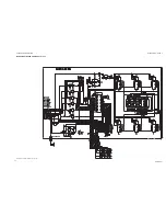
2.7
KEYBOARD UNIT MODULE 7/700
2.7.1
DISPLAY
The LCD-display is static driven with an 50 Hz AC signal measured with reference to the back plane input
(BP pin numbers 1, 27, 28, 54). A segment that is off always has the same voltage as the BP. The latches
(U1-7 - U6-7) is loaded serially from the µC. Every 10 mS a strobe pulse is sent to the latches, and the
content of the internal shift register in the latches is loaded into the output latches. Afterwards new
information is shifted into the shift registers so the content is ready when the next 10 msec cycle has
passed.
2.7.2
KEYBOARD
The keyboard is scanned once every 10 mS. First PA4 is turned low, and PAO- PA3 are turned into inputs.
Afterwards PCO-PC3 are read, and if there is a low level on one of these pins a push button is activated.
If they are all high PA3 is turned low and the others to input pins, and PCO-PC3 are read once more and
so on. When finished PAO is left at low level.
2.7.3
PANEL ILLUMINATION
The LEDs are driven with a constant current generator. With PB1 at OV the current generators are on
and with PB1 at 5V they are switched off.
2.7.4
THE MICROCOMPUTER
The µC uses the internal clock-generator and a ceramic resonator. The clock frequency is approx. 4 MHz.
The µC takes care of the dual watch and scanning functions and the keyboard and display. This means
that when scanning, the µC requests a new channel every 100 mS if it has not received a message telling
that there is a carrier. Concerning the serial interface see section 2.6.14 COMMUNICATION BETWEEN
THE TWO µC’S. When the radio is on and the ON/OFF switch is activated and released again the µC will
be interrupted. The µC will then transmit a message to U19-6 to tell it to switch off. C18-7 and R17-7 is
an external pullup of the RESET
*
-pin and keeps the RESET
*
set for 0.5 second after the set is turned off
allowing time for transferring the startup table to the Interface µC. The interface µC then stores this
information in the eeprom before the set is finally turned off.
2.7.5
THE SP VHF-BUS
The keyboard µC also handles the communication with external units on the SP VHF Bus. The structure
is a digital Command/Response time division multi-pleasing data bus, with an interrupt extension. The
interrupt signal is located on pin 23 (PC5) on the µC and the serial I/O signals on pin 29/30 (PD0/PD1).
The RT2047 will always behave as a slave in the communication but can initiate a dialogue with the
external unit by setting the interrupt pin. A communication sequence will typically be initiated by the
external unit ( the master ) with an Address Word specifying what slave it wants to contact, a Command
Code or a Transfer Code ordering the slave to execute a command or to transfer information to the master
and finally a number of Data Words. The number of data Words can vary from 0 to 10. The answer from
the slave (RT2047) could consists of a Status Word, specifying what slave the answer came from and
a Response Word confirming that the command has been executed, optionally a Message Code and a
number of Data Words corresponding to the data transfer requested by the master. The answer from the
slave could also consist of a Status Word with its Busy-bit set and a Response Word confirming that the
command was received. In this case the slave will set the interrupt pin when it’s ready and the following
communication will confirm that the command was executed or optionally give the data transfer
requested. There are several other types of communication. For these and for specifics we refer to the
documentation on the SP VHF-BUS.
PAGE 2-24
9543
Summary of Contents for RT2047
Page 1: ...S P RADIO A S AALBORG DENMARK TECHNICAL MANUAL FOR COMPACT VHF RT2047 D ...
Page 2: ......
Page 5: ...RT2047 DSC PART I CONTENTS 1 GENERAL INFORMATION 1 1 1 1 INTRODUCTION 1 1 ...
Page 6: ......
Page 8: ......
Page 10: ......
Page 24: ......
Page 30: ...1 GENERAL INFORMATION RT2047 DSC PART II PAGE 1 6 9543 ...
Page 32: ......
Page 34: ......
Page 46: ...2 CIRCUIT DESCRIPTION RT2047 DSC PART II PAGE 2 12 9543 ...
Page 50: ...2 CIRCUIT DESCRIPTION RT2047 DSC PART II 9543 PAGE 2 16 ...
Page 66: ...9546 ...
Page 67: ...2 CIRCUIT DESCRIPTION RT2047 DSC PART II 9546 PAGE 2 33 32162 ...
Page 81: ......
Page 82: ......
Page 84: ......
Page 86: ...3 MECHANICAL DISASSEMBLING AND MODULE LOCATION RT2047 DSC PART II PAGE 3 2 9545 ...
Page 88: ......
Page 90: ......
Page 98: ...4 SERVICE RT2047 DSC PART II PAGE 4 8 9545 ...
Page 99: ...4 SERVICE RT2047 DSC PART II 4 11 PIN CONFIGURATION 9545 PAGE 4 9 ...
Page 109: ...RT2047 DSC PART II CONTENTS 5 PARTS LISTS 5 1 9546 ...
Page 110: ......
Page 124: ......

