background image

Module Descriptions, RFL 9508D RF Section 


7.9


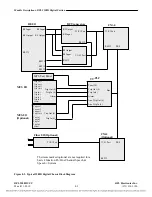
RFL 9508D RF MOTHER BOARD 


FOR JUMPER SETTINGS ON REVERSE 
SIDE OF BOARD SEE FIGURE 5-22

RX OUT 

4W RX 

4W TX 

OR 2W I/O 

EXT AMP IN

TX IN 

EXT AMP 

OUT 

EXT AMP 

FAIL IN

ATTENUATOR 

BOARD 

NOTE: Dotted lines indicate boards that plug into the motherboard from the front of the RFL 9508D chassis. 

NC 

NO 

NC 

NO 

CHASSIS GND 

EARTH GND 

INT 
AMP 
FAIL 


EXT 
AMP 
FAIL 

RX FILTER 


LINE BOARD 

BALANCE 

BOARD 

TX FILTER 


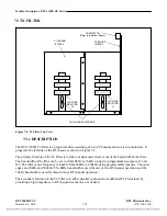
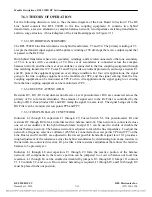
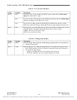
Figure 7-14. RFL 9508D RF Motherboard, rear view 


7.9.1


DESCRIPTION 


The RFL 9508D RF Motherboard is a 4.5 x 8 inch assembly, which is mounted on the rear right side of the 
9508D chassis as viewed from the front. It provides interconnections for the five RF modules that plug into 
it from the front of the chassis, which are the TX Filter, Balance Board, Line Board, Attenuator Board, and 
Rx Filter. Figure 7-14 shows the rear view of the motherboard. Connectors J6 and J7 are TNC connectors 
which provide connections to the line coupling equipment. J4, J5, J8 and J9 are BNC connectors, J10 is a 
two pin plug-in connector, and TB1 is an eight position terminal block. 


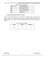
Table 7-3. Motherboard Rear Panel Connector Assignments 


Board Label 

Reference 
Designation 

Connector type 

Application 

TX IN 

J1 

BNC 

Tx In from MA-650 

EXT AMP IN 

J5 

BNC 

Input signal from external amp 

EXT AMP OUT 

J3 

BNC 

Output signal to external amp 

4W RX 

J6 

TNC 

4W Input from line coupling equipment 

4WTX OR 2WI/O 

J7 

TNC 

4W Output to line coupling equipment or 2W Input/Output 

RX OUT 

J8 

BNC 

Rx Out to MA-650 

EXT AMP FAIL IN 

J10 

Two-pin plug-in type 

External Amp Fail input 

INT AMP FAIL 

TB1 

8-position terminal block 

Power Amplifier Fail, Relay Contacts 

EXT AMP FAIL 

(See Table 7-4 for TB1 terminal assignments) 

RFL 9508D UCC 


RFL Electronics Inc. 

December 1, 2010 

7-17 

         (973) 334-3100


Summary of Contents for 9508D UCC

Page 1: ...o revise this manual and make changes to its contents from time to time We assume no liability for losses incurred as a result of out of date or incorrect information contained in this manual RFL Elec...

Page 2: ...ay shipping cost of the failed assembly to the RFL Customer Service facility in Boonton New Jersey RFL warrants product repair from one year from the date of repair or the balance of the original fact...

Page 3: ...n o t i c e WARNING LABELS AND SAFETY SUMMARY FOR YOUR SAFETY THE INSTALLATION OPERATION AND MAINTENANCE OF THIS EQUIPMENT SHOULD ONLY BE PERFORMED BY QUALIFIED PERSONS CAUTION WARNING RFL 9508D UCC R...

Page 4: ...OM LIVE CIRCUITS Operating personnel should never remove covers Component replacement and internal adjustments must be done by qualified service personnel Before attempting any work inside the product...

Page 5: ...READY TO BE INSTALLED WARNING YOUR RFL 9508D TERMINAL MAY BE EQUIPPED WITH FIBER OPTIC INPUT OUTPUT MODULES THAT HAVE FIBER OPTIC EMITTER HEADS FIBER OPTIC EMITTER HEADS USE A LASER LIGHT SOURCE THAT...

Page 6: ...UCC 2 10 SECTION 3 INSTALLATION 3 1 3 1 INTRODUCTION 3 1 3 2 UNPACKING 3 1 3 3 MOUNTING 3 2 3 4 VENTILATION 3 5 3 5 CONNECTIONS 3 6 SECTION 4 RFL NETWORK MANAGEMENT SOFTWARE 4 1 4 1 GENERAL INFORMATI...

Page 7: ...cs Inc September 7 2012 vii 973 334 3100 8 3 CM4 OPTICAL INTERFACE ADAPTERS 8 23 8 4 PLC TRANSFER TRIP MODULE 8 26 8 5 PLC TRANSFER TRIP MODULE ADAPTERS 8 30 8 6 TELEPROTECTION ANALOG AND DIGITAL TRAN...

Page 8: ...window 4 19 Figure 4 16 CM4 configuration window 4 22 Figure 4 17 Configuration parameters for PLC TT card 4 24 Figure 4 17 PLC TT card s status window 4 28 Figure 5 1 Front View Of RFL 9508D Chassis...

Page 9: ...508D Digital Chassis showing insertion of modules and module adapters 8 6 Figure 8 5 RFL 9508D Digital Chassis showing Power Supply and CM4 front panel switches indicators and jacks 8 7 Figure 8 6 Fro...

Page 10: ...on the Transceiver module 5 25 Table 5 14 Analog Chassis Jumper Configurations And Other Settings 5 28 Table 5 15 Function of jumpers connectors and potentiometers on Power Amp 5 30 Table 5 16 Functio...

Page 11: ...EFFECTIVE PAGES When revisions are made to the RFL 9508D UCC Instruction Manual the entire section where revisions were made is replaced For the edition of this manual dated September 7 2012 the sect...

Page 12: ...xii 973 334 3100 REVISION RECORD Rev Description Date Approval 7 1 07 New Document Release 7 1 07 TG 3 11 10 Updates to Section 3 4 5 6 and 8 Ref CAR 9508 0210 3 11 10 TG 10 18 10 Sections 5 6 and 7...

Page 13: ...n u o u s p r o d u c t i mp r o v e me n t wer e s e r v et h er i g h t t oc h a n g ed e s i g n s a n ds p e c i c a t i o n s wi t h o u t n o t i c e Product Information RFL 9508D UCC RFL Electr...

Page 14: ...o u s p r o d u c t i mp r o v e me n t wer e s e r v et h er i g h t t oc h a n g ed e s i g n s a n ds p e c i c a t i o n s wi t h o u t n o t i c e Product Information This page intentionally lef...

Page 15: ...The RFL 9508D UCC comprises two integrated subsystems that consist of a highly integrated fully digital PLC terminals that incorporates the latest Digital Signal Processing technology DSP along with...

Page 16: ...configure the system requirements SNMP alarm reporting traps are also supported if required The RFL 9508D UCC can be accessed via RS 232 interface or remotely with an optional Ethernet access port Sys...

Page 17: ...are found inside the front panel Line TX after transmit filter Line RX before front end filter and Line after the Hy brid These signals facilitate equipment testing and com missioning The Skewed Hybri...

Page 18: ...802 3 SNAP Network Management SNMP management via Network Management Sys tem NMS Menu driven async console port VT 100 via DB9 male connector auto sensing DTE DCE Remote Telnet access to command port...

Page 19: ...otection via Optic Link Many times the protective relays are not located in the same building as the communications systems that are used to transmit the relaying signals A unique feature of the RFL 9...

Page 20: ...odulation FSK Frequency shift 30 Hz from channel center frequency Technical Specifications Additional Features Selectable Unblock Logic In the event that the receiver enters an alarm state the out put...

Page 21: ...n B Channel separation by echo cancellation techniques C QuadratureAmplitude Modulation QAM for each channel with synchronous line transmission at selectable symbol rates of 2400 3000 3200 3429 symbol...

Page 22: ...o u s p r o d u c t i mp r o v e me n t wer e s e r v et h er i g h t t oc h a n g ed e s i g n s a n ds p e c i c a t i o n s wi t h o u t n o t i c e RFL 9508 RFL Electronics Inc June 2005 8 Specifi...

Page 23: ...o l i c yo f c o n t i n u o u s p r o d u c t i mp r o v e me n t wer e s e r v et h er i g h t t oc h a n g ed e s i g n s a n ds p e c i c a t i o n s wi t h o u t n o t i c e RFL 9508 RFL Electron...

Page 24: ...v et h er i g h t t oc h a n g ed e s i g n s a n ds p e c i c a t i o n s wi t h o u t n o t i c e RFL 9508 RFL Electronics Inc June 2005 10 RFL 9508D UCC September 2007 Notes 1 Base UCC system inclu...

Page 25: ...l i c yo f c o n t i n u o u s p r o d u c t i mp r o v e me n t wer e s e r v et h er i g h t t oc h a n g ed e s i g n s a n ds p e c i c a t i o n s wi t h o u t n o t i c e RFL 9508 RFL Electroni...

Page 26: ...l l h a v eap o l i c yo f c o n t i n u o u s p r o d u c t i mp r o v e me n t wer e s e r v et h er i g h t t oc h a n g ed e s i g n s a n ds p e c i c a t i o n s wi t h o u t n o t i c e RFL 950...

Page 27: ...ge impedance of the power line to the impedance of the 9508D terminal The LTU also contains a surge arrestor to protect the equipment from voltage spikes lightning or other faults The coupling capacit...

Page 28: ...h t t oc h a n g ed e s i g n s a n ds p e c i c a t i o n s wi t h o u t n o t i c e Applications RFL 9508D UCC RFL Electronics Inc 9508D 9508D PACKET MUX PACKET MUX LTU LTU PLC TT RTU 21P B A A B 21...

Page 29: ...oint to point voice channel or as a autodial extension so other extensions Node A for example can dial to this locations Each 9508D terminal is connected to the power line via an LTU Line Tuning Unit...

Page 30: ...t i o n s wi t h o u t n o t i c e Applications RFL 9508D UCC RFL Electronics Inc 9508D LTU 21P A B A PABX SCADA MASTER LTU LTU C LTU PLC TT FXO B 21P B A ARD 21P B C ETHERNET PLC TT RTU 21P C B 9508...

Page 31: ...ns are single tone only and are typically used for blocking or permissive underreach or permissive overreach Coded signal transmissions have two alternating tone frequencies and are typically used for...

Page 32: ...utputs 1 2 3 and 4 on the PLC TT I O adapter module Table 2 3 Preset Frequencies F number Frequency Notes F1 427Hz Test signal frequency F2 640Hz Trip signal frequency F3 853Hz Trip signal frequency F...

Page 33: ...utputs 4 Inputs PLC TT I O PLC TT 4 Inputs 4 Outputs Figure 2 3a Typical Configuration Figure 2 3b Dual I O Configuration Note 1 In Figures 2 3a and 2 3b the outputs can be Inverted or Not Inverted us...

Page 34: ...eration The analog filters are fully adjustable in this range in 2 KHz steps As their bandwidths are significantly wider than the channel bandwidth they do not need finer adjustment 2 4 SUPERPOSED SEP...

Page 35: ...ones within the bandwidth of the RX filter so it does not provide any additional rejection The RX filter in the 9508D can be set to two channel widths For single channels RFL recommends the use of a f...

Page 36: ...f the NMS as shown in Figures 4 22 and 4 24 For the standard applications the RX filter is set to 8 KHz 2 8 LINE BOARD The Line Board is the interface between the RFL 9508D UCC and the line coupling e...

Page 37: ...that reason the peak to average relation of a QAM signal must be considered when setting the amplifier gain ABSOLUTE RECEIVE LEVEL 1 After the hybrid is balanced the absolute receive level into the t...

Page 38: ...i n u o u s p r o d u c t i mp r o v e me n t wer e s e r v et h er i g h t t oc h a n g ed e s i g n s a n ds p e c i c a t i o n s wi t h o u t n o t i c e Applications This page intentionally left...

Page 39: ...e RFL 9508D UCC including unpacking mounting and interconnection wiring Refer to Table 3 4 at the end of this section for a list of modules used in the RFL 9508D UCC 3 2 UNPACKING RFL 9508D UCC equipm...

Page 40: ...carefully examine all packing materials to make sure no items of value are discarded 3 Carefully remove any packing materials that were inserted into the individual chassis to hold circuit cards in pl...

Page 41: ...o t i c e Installation 0 187 in 0 475 cm DIA 8 REQ 2 25 in 5 715 cm 1 5 in 3 81 cm CUTOUT 17 625 in 44 768 cm 18 312 in 46 512 cm 10 5 in 26 67 cm 3 0 in 7 62 cm 2 25 in 5 715 cm CUTOUT 17 625 in 44...

Page 42: ...lower chassis 4 REQ for upper chassis 2 25 in 5 715 cm 1 5 in 3 81 cm CUTOUT 17 625 in 44 768 cm 18 312 in 46 512 cm 10 5 in 26 67 cm 3 0 in 7 62 cm 2 25 in 5 715 cm CUTOUT 1 5 in 3 81 cm 2 25 in 5 7...

Page 43: ...or cabinet 2 Remove all the screws securing the shipping rails to the equipment 3 Slide the equipment into the rack or cabinet 4 Install and tighten screws to all panels to secure the equipment in pl...

Page 44: ...spade lugs depending on local practice To connect wires to the terminal blocks proceed as follows 1 Remove the transparent protective cover from the rear of the chassis by loosening the mounting screw...

Page 45: ...ween the RFL 9508D UCC and the Line Coupling Equipment Signal Name From To High Level Power I O 2W I O Line Coupling Equipment EXTERNAL CONNECTIONS FROM RF CHASSIS TO DIGITAL CHASSIS The following con...

Page 46: ...9508D UCC chassis is the main ground for the RFL 9508D UCC terminal This can be seen in Figures 3 3 and 3 4 Grounding is accomplished by connecting a wire 6AWG or larger between this ground stud and...

Page 47: ...IL EXT AMP FAIL IN EXT AMP FAIL IN on upper RF chassis on lower RF chassis EXT AMP IN EXT AMP IN EXT AMP IN on upper RF chassis on lower RF chassis EXT AMP OUT EXT AMP OUT TX IN on lower RF chassis on...

Page 48: ...nected to an external loop current generator 1 RG RING GEN For connection to an external ring generator referenced to SIG BAT Connect one side of the ring generator to the RING GEN terminal and the ot...

Page 49: ...5770 4 IN IN TRIP4 TRIP3 OUT OUT IN IN TRIP2 TRIP1 OUT OUT C NC NO ALARM MA 470 V 35 TX RX CRAFT INT AMP FAIL EXT AMP FAIL FROM TO LINE COUPLING EQUIPMENT V V C NO NC PC or LAPTOP 1 0 1 0 P S DIGITAL...

Page 50: ...IP3 OUT OUT IN IN TRIP2 TRIP1 OUT OUT C NC NO ALARM RX OUT J 4W TX OR 2W I O EXT AMP IN TB1 TX IN EXT AMP OUT EXT AMP FAIL IN C NC NO C NC NO CHASSIS GND EARTH GND 4W RX INT AMP FAIL EXT AMP FAIL FROM...

Page 51: ...t i c e Installation 4TT I O 48 125V 105770 4 IN IN TRIP4 TRIP3 OUT OUT IN IN TRIP2 TRIP1 OUT OUT ALARM PC or LAPTOP 1 0 1 0 P S DIGITAL P S RF COM NC NO COM NC ON OFF F1 6A F2 6A ON OFF RF RF SB RG...

Page 52: ...Transceiver 107830 D F 5 2 1 9 5 3 1 6 8 6 Digital Transceiver D F 5 2 1 10 5 3 1 7 8 7 MA 271 I O 107295 D R 5 2 1 5 5 3 1 2 8 2 MA 278 I O 107475 D R 5 2 1 5 5 3 1 2 8 2 Optical I O 107455 201 to 60...

Page 53: ...es the user to communicate with all 9508D terminals located in a network 2 Enables the user to access information regarding the configuration of any node in the network 5 Enables the user to customize...

Page 54: ...o 999 2 Before loading the software make a working copy of the CD Store the original CD in a safe place and use the working copy to load the software into the PC 3 Before installing the software it is...

Page 55: ...appear on the screen If not do the following a From the Start Menu select Run b The Run window will appear on the screen c Type the following in the command line d RFL9508D_setup exe d is considered a...

Page 56: ...stall or change remove button This will cause the Uninstall program to permanently erase all of the programs icons directories and files related to the RFL 9508D Network Management Software from your...

Page 57: ...onnection over a public or private phone line as shown in Figure 4 4 Either of the two ways of connection to the equipment lets the user to read the configuration and change specific settings on the r...

Page 58: ...L Network Management Software 9508D CHASSIS CRAFT MA 470 TRANSCEIVER a Connecting a PC to the MA 470 Craft Port PC RS 232 COM PORT NODE Figure 4 3 PC directly connected to a node using an RS 232 cable...

Page 59: ...CABLE COM LOCAL NODE 9508D CHASSIS MA 470 TRANSCEIVER REMOTE NODE POWER LINE Figure 4 5 Remote configuration of a PLC terminal PC COM PORT MA 470 CABLE DB 9 MALE DB 9 FEMALE NC XMIT DATA OUTPUT REC D...

Page 60: ...of the four nodes is connected via a different communication path Figure 4 8 shows a PC at a remote location connected to 2 nodes where all nodes are in the same network The nodes communicate Network...

Page 61: ...e s i g n s a n ds p e c i c a t i o n s wi t h o u t n o t i c e RFL Network Management Software POWER LINE Null modem cable may be required RS232 cable PHONE LINE 1 NODE 2 MODEM MODEM NODE 1 PC Fig...

Page 62: ...ork is connected to another node allowing communication to pass from one node to another The communication path must have a beginning and an end as shown in Figure 4 9 Each box represents a node in th...

Page 63: ...nsceiver 9508D Terminal CM4 PLC TT Transceiver 9508D Terminal 4 4 1 STARTING THE NETWORK MANAGEMENT SOFTWARE To start the Network Management Software click on the RFL9508D UCC NMS Icon on your desktop...

Page 64: ...al 1 Type in a name for the unit in the device location field 2 Select a communications mode from the available options in the pull down box 3 If necessary type in an IP address used when configuring...

Page 65: ...ure 4 12 RFL9508D UCC NMS presentation window Note that this window has four top level pages selected by tabs near the top of the window as follows Digital XCVR Analog XCVR CM4 and PLC TT The digital...

Page 66: ...discussed in the following paragraphs 1 Write DPLC This button is used to start a write operation of all the parameters in the Common and Digital channel tabs to the DPLC transceiver 2 Read DPLC This...

Page 67: ...s pressed it toggles between local and remote mode for a link to be established one end must be configured as local and the other end as remote 3 Tx Pilot High and Rx pilot High To setup a digital cha...

Page 68: ...eter is set to 200 KHz 10 Rx Frequency Through this pull down box you can select the receive band s lower edge frequency For example if the receive stream occupies from either 104 to 108 KHz or 104 to...

Page 69: ...ettings window The settings configured at this window are described below 1 NMS Access The read and or write operations will be performed over the local or remote teleprotection transceiver as selecte...

Page 70: ...elect the receive band s lower edge frequency of the teleprotection channel The teleprotection channel is always 4 KHz wide therefore this RX frequency should be set consistently according with the Di...

Page 71: ...sceiver show memory maps and teleprotection show memory maps Note This button is only available when logged as an administrator 4 Address Discovery Pressing this button the software will start an addr...

Page 72: ...uration this parameter is set to 1 5 5 Nominal Gain Can be set from 0 to 100 dB This value should be set during commissioning to the same value of the current transceiver gain obtained through the mon...

Page 73: ...ded TEV ms Can be set from 0 00ms to 63 00ms in 0 25ms steps This is also referred to as the signal evaluation time The signal evaluation time should be set to factory recommended value of 12 00ms dir...

Page 74: ...or button is pressed a message will be displayed in the Channel 1 Status box An example of a message in the Channel 1 Status box is as follows Current Gain 18dB Nominal Gain Reference 10dB Rx Signal v...

Page 75: ...nc with PC and after a Write operation the date and time will be updated in the CM4 with the date and time settings from the PC where the configuration software is running The module uses this date an...

Page 76: ...r Inverted 2 Input 1A Polarity Input 1A Polarity can be set to Normal or Inverted 3 Input 2 Polarity Input 2 Polarity can be set to Normal or Inverted 4 Input 2A Polarity Input 2A Polarity can be set...

Page 77: ...p timer can be set from 0 00ms to 4 00ms in 0 25ms increments Select the pretrip timer value that you want from the pull down box 0 25ms to 4 00ms are valid 15 Func 3 pretrip timer ms The Function 3 p...

Page 78: ...e triphold timer value that you want from the pull down box 27 Func 3 triphold timer ms When a trip is received it will extend the trip 3 by the time selected The Function 3 triphold timer can be set...

Page 79: ...to 2550 00ms in 10ms increments Select the Alarm time delay that you want from the pull down box 36 Trip Reset Counter The Trip Reset Counter can be set to Run or Reset When set to Reset all trip coun...

Page 80: ...PLC TT card s status window When the update button is pressed the window is refreshed with status values from the PLC TT card these values include the Trip input output counters and a list of the new...

Page 81: ...the field It is assumed that the installation procedures described in Section 3 of this manual have been performed and the 9508D chassis are in place Figure 5 1 shows the location of the RFL 9508D fr...

Page 82: ...al LED green LED is ON when there are no system ALERT or ALARM conditions in the AF chassis 4 Alert LED amber LED is ON See Table 8 2 Item 5 5 Alarm LED red LED is ON See Table 8 2 Item 6 6 RF Chassis...

Page 83: ...wer Supply 5 2 1 1 Redundant Power Supply 5 2 1 2 Power Supply Alarm I O 5 2 1 3 CM4 Optional Module 5 2 1 4 MA 271 MA 278 or Optical I O 5 2 1 5 PLC Transfer Trip 5 2 1 6 One or two PLC Transfer Trip...

Page 84: ...Terminal End or Drop and Insert A DI A applications If a second CM4 is used it must be installed in the front of the chassis in slot 1 This is the Optional Common Module The CM4 in slot 1 is used for...

Page 85: ...odule adapters One in slots 5 through 7 The other in slots 11 through 13 A cable is required from slot 8 of the motherboard to JP3 of The PLC TT Module One 4 function module adapter Slots 5 through 10...

Page 86: ...G TELEPROTECTION TRANSCEIVER TEST PANEL SEE NOTE 1 CM4 OPTIONAL CM4 MAIN PLC TT MODULE MAIN POWER SUPPLY REDUNDANT POWER SUPPLY MA 470 FRONT REAR MOTHER BOARD POWER SUPPLY ALARM I O MA 271 MA 278 OR O...

Page 87: ...he Transceiver module requires a Module Adapter The Module Adapter used with the Transceiver Modules is the MA 470 which is mounted at the rear of the chassis directly behind the Transceiver Modules D...

Page 88: ...Section Module placement in the RF Chassis is shown in Table 5 4 and Figures 5 4 and 7 1 A Typical RF Chassis will have modules installed as indicated in Figure 5 4 Table 5 4 Module Placement In RF Ch...

Page 89: ...the 6U chassis and the Balance Board without components is installed in the 3U chassis for 100W operation LINE BOARD The Line Board is a module which plugs into a slot in the RF Mother Board immediate...

Page 90: ...re shown pictorially in Figure 5 5 Table 5 5 9508 RF Chassis Cables RFL cable part number From To Function 107806 2 of 2 J1 of Power Amp Power Supply J1 of Power Amp 3 conductor cable which provides d...

Page 91: ...h t t oc h a n g ed e s i g n s a n ds p e c i c a t i o n s wi t h o u t n o t i c e Configuration J1 REAR VIEW OF POWER AMP POWER SUPPLY Rear View of RF Chassis Motherboard Rear View of Power Ampli...

Page 92: ...e lower 6U chassis and the upper 3U chassis for convection cooling The 3U chassis will contain a 50W Power Amplifier a Power Amp Power Supply a Tx Filter an External Amp Connection Board and a Motherb...

Page 93: ...LY ALARM I O 4 FUNCTION PLC TT MODULE ADAPTER A 4 FUNCTION PLC TT MODULE ADAPTER B Figure 5 7 Module placement for 9508RT 5 2 7 MODULE PLACEMENT IN THE PACKETIZING MULTIPLEXER The packetizing multiple...

Page 94: ...T Interface Card 5 2 7 9 Dual Serial Port Interface Card 5 2 7 10 5 2 7 1 5 2 7 2 5 2 7 3 DUAL QUAD FXS INTERFACE CARD It provides a subscriber line connection to a conventional two wire analog teleph...

Page 95: ...lled in another slot a T1 E1 interface card can be installed in place of the T1 Interface card then the T1 E1 card can be configured for T1 operation T1 E1 INTERFACE CARD This is a dual port interface...

Page 96: ...multiplexer according to data traffic needs It has 2 universal serial ports per interface card supporting V 35 V 11 TIA 232 V 24 X 21 X 21 CE TIA 449 V 36 and TIA 530 interfaces The connector used is...

Page 97: ...e Configuration 5 3 1 1 SETTING JUMPERS ON THE CM4 MODULE The CM4 Common Module has four sets of jumpers that must be set for proper system operation These are J3 J4 J6 and J8 and are shown in Figure...

Page 98: ...you are setting up is located in chassis slot 10 J6 jumpers should be installed as follows If the CM4 you are setting up is for DI A or Terminal the two upper J6 jumpers should be installed The two lo...

Page 99: ...anel views and pinouts J3 Application RFL 9508D UCC RFL Electronics Inc U Place jumper in U position to unground the outer conductor of the Receive Port RX IN This is the normal position for this jump...

Page 100: ...rface adapters have two switches that must be set for proper system operation These are shown in Figure 5 10 and described Table 5 8 below See Figure 8 9 for a panel view and pinouts The CM4 installed...

Page 101: ...5 10 Setting Jumpers on the PLC TT module Jumper Function J1 connector For factory use only J2 jumper Enables or disables the watchdog timer Used for factory testing only Should always be in RUN DOWN...

Page 102: ...to set these jumpers 125V 48V 125V 48V INPUT TERMINAL BLOCK J5 J4 For 48V OPERATION JUMPERS SHALL BE LOCATED AS SHOWN Figure 5 13 Location and use of voltage control jumpers on a typical I O adapter...

Page 103: ...or 125V operation 105740 4 105770 3 2 function 250V solid state 105770 5 4 function 250V solid state 125V position 105740 3 2 function 250V relay for 250V operation 105740 5 4 function 250V relay 5 3...

Page 104: ...power is applied to transceiver module D2 Channel 0 Status Has three states as follows GREEN No alarms detected on Channel 0 Flashing RED Signal to Noise ratio is below the threshold The threshold is...

Page 105: ...is all test points are for factory use only The Transceiver Module has 5 LEDs as follows D1 through D5 The location of these LEDs is shown in Figure 5 13 The function of the LEDs is shown in Table 5 1...

Page 106: ...Transceiver Modules and provides the appropriate connections to the line coupling equipment and the packetizing multiplexer This Module Adapter has two jumpers one jumper JP1 that must be set to eithe...

Page 107: ...OP AND INSERT APPLICATIONS In T1 E1 applications the RFL 9508D can be either Terminal DI A or DI B Several of the modules in the 9508D chassis have jumpers that must be set to select Terminal or Drop...

Page 108: ...3 2 6 5 3 2 1 SETTING JUMPERS AND SWITCHES ON 50W POWER AMPLIFIER The 50W Power Amplifier has a circuit board which contains two programmable jumpers J6 and J7 In addition to this the board has five...

Page 109: ...J3 DS1 SW1 SW2 Top View Switch Block Typical ON 1 2 3 4 SW2 5 6 7 8 Figure 5 17 Circuit board of the 50W Power Amp showing locations of jumpers switches connectors potentiometers As shown above effect...

Page 110: ...hich set the outputs of the two 50W amplifiers 180 deg out of phase This will insure that the total output power is additive In 50W applications J6 and J7 can be set either way In 100W applications on...

Page 111: ...through SW1 8 can be set as follows Note that SW1 2 SW1 4 SW1 5 and SW1 6 are not used DIP Switch Phase Angle in Degrees SW1 1 30 SW1 3 45 SW1 7 60 Default setting SW1 SW1 8 90 Phase Detector Set Poin...

Page 112: ...two large air core inductors The location of these jumpers is shown in Figure 5 17 The remaining 17 Jumpers are located on the 107828 1 board The location of these jumpers is shown in Figure 5 18 Ref...

Page 113: ...ng to your configuration If needed spare jumpers are shipped with each unit 4 Set the 8kHz 16kHz bandwidth jumper to the appropriate position 5 Using the RFL 9508D NMS software set the Transceiver to...

Page 114: ...es capacitance may have to be varied use the schematic as a guide 11 Set Jumper J44 in the TEST position 12 Adjust L2 left coil for a minimum level on the meter The coil is adjusted by turning the pla...

Page 115: ...o u t n o t i c e Configuration CONNECTOR Plugs Into Mother Board PC BOARD 107828 2 PC BOARD 107828 1 AIR CORE INDUCTOR L2 AIR CORE INDUCTOR L1 J31 J33 J30 J34 J35 J32 J38 J39 J40 J41 J42 J43 J36 J37...

Page 116: ...r v et h er i g h t t oc h a n g ed e s i g n s a n ds p e c i c a t i o n s wi t h o u t n o t i c e Configuration J44 J1 NORMAL TEST 16kHz 8kHz J17 J16 J15 J12 J13 J11 J7 J6 J5 J10 J4 J3 J2 J9 J8 Fi...

Page 117: ...J2 J3 and J4 that must be set for proper system operation The jumper settings select either 50W or 100W operation and must be set in accordance with Table 5 17 The jumper locations are shown in Figur...

Page 118: ...system operation Two of these jumpers J10 and J20 are for impedance matching 12 jumpers are used for balancing the line impedance and 4 jumpers are used to select 2W or 4W operation The location of th...

Page 119: ...various resistors to adjust the resistive component of the line impedance Refer to the Hybrid Tuning procedure in paragraph 6 2 5 1 J28 Jumper Install this jumper in the TOP position if the attenuator...

Page 120: ...100 that must be configured for proper system operation These jumpers allow a user to select the bandwidth which can be either 8kHz or 16kHz and to tune the center frequency which can be from 24kHz to...

Page 121: ...ection Phillips head core alignment tool for L1 L2 and L3 9508 RF Extender Card RX Filter Tuning Procedure 1 Turn Power OFF to the RF and AF Chassis of the 9508D 2 Use RFL 9508D NMS software to genera...

Page 122: ...L3 to have minimum loss at center frequency The final level measurement is called the OFFSET 9 Set TX Frequency according to step 7 to RX filter center frequency 4 kHz for 8kHz bandwidth or 8kHz for 1...

Page 123: ...et h er i g h t t oc h a n g ed e s i g n s a n ds p e c i c a t i o n s wi t h o u t n o t i c e Configuration RFL 9508D UCC RFL Electronics Inc JB GROUP JC GROUP JL2 GROUP JE GROUP JD GROUP JA GROU...

Page 124: ...f Jumpers on RF Motherboard 5 3 2 7 5 3 2 8 5 3 2 9 SETTING JUMPERS ON THE RF MOTHERBOARD There are two jumpers on the RF Mother Board J13 and J14 Set to A for unbalanced tied to ground and set to B f...

Page 125: ...ms require jumpers to be set on the Balance Board as follows J2 must be set to the 2 3 position J3 must be set to the 1 2 position J4 must be set to the 1 2 position Refer to paragraph 5 3 2 3 and Fig...

Page 126: ...n u o u s p r o d u c t i mp r o v e me n t wer e s e r v et h er i g h t t oc h a n g ed e s i g n s a n ds p e c i c a t i o n s wi t h o u t n o t i c e Configuration This page intentionally left...

Page 127: ...R MUST BE TERMINATED PROPERLY BEFORE BEING ENERGIZED FAILURE TO DO THIS MAY RESULT IN DAMAGE TO THE TX FILTER SEE STEP 4 BELOW CAUTION THE POWER AMPLIFER WILL SHUTDOWN IF NOT PROPERLY TERMINATED CONDU...

Page 128: ...sion won t need a password for administrator privileges type in ok and press ENTER 6 2 3 9508D NMS SOFTWARE ACCESS 1 Copy Configuration files from the system CD supplied with the equipment 2 Load the...

Page 129: ...ct the CM4 tab k Press the Discovery button at the top of the page l Press the Read button at the Bottom of the page m Select the PLC TT Tab n Press the Read button o Select the File Toolbar p Select...

Page 130: ...t a 50 ohm non inductive dummy load of sufficient wattage 50 100 to the carrier output connector 4W Tx or 2W I O RX OUT J 4W TX OR 2W I O EXT AMP IN TX IN EXT AMP OUT EXT AMP FAIL IN C NC NO C NC NO E...

Page 131: ...s across the dummy load and verify the following approximate levels as applicable for your system 50 Watts system 38 dBm 2 dB 100 Watts system 41 dBm 2 dB 6 Adjust using R83 on the amplifier card if n...

Page 132: ...J15 J17 J18 J19 J21 and J22 IN until a combination of inductance provides a minimum reading on the FSVM 14 Repeat steps 11 above until lowest level is attained 15 Repeat steps 1 to 15 in Section 6 fo...

Page 133: ...Refer To The Following Paragraphs 50W Power Amplifier 105085 7 1 Power Amp Power Supply 107250 4 5 7 2 Tx Filter 107825 7 3 Balance Board 107815 7 4 External Amp Connection Board 107870 7 5 Line Boar...

Page 134: ...o d u c t i mp r o v e me n t wer e s e r v et h er i g h t t oc h a n g ed e s i g n s a n ds p e c i c a t i o n s wi t h o u t n o t i c e Module Descriptions RFL 9508D RF Section RFL 9508D UCC RFL...

Page 135: ...FILTER POWER SUPPLY 50W POWER AMP BATTERY BATTERY PWR FAIL COM PWR FAIL NO PWR FAIL NC 92V 30V GND TB1 1 TB1 2 TB1 3 TB1 4 TB1 5 92V 30V GND SIGNAL IN GND FAIL OUT SIGNAL OUT ALARM RELAY ALARM RELAY_...

Page 136: ...develops an RF output of 50 Watts A green LED is located on the left side of the Power Amplifier front panel as shown in Figure 7 3 The LED is ON when the power amplifier is transmitting In those appl...

Page 137: ...e subject to change without notice Number Of Inputs Two Input Level 10 dBm 75 Ohms single input 4 dBm 75 Ohms two inputs Input Impedance 50 Ohms nominal Idle Noise 65 dBmO measured in a 3 kHz bandwidt...

Page 138: ...RFL 9508D PACKETIZING MUX 1U Minimum Space POWER NORMAL ALERT ALARM RFL 9508D AF CHASSIS RFL Electronics Inc Additional 3U Chassis For 100W Systems POWER NORMAL ALERT ALARM RFL 9508D AF CHASSIS RFL El...

Page 139: ...erent types of Power Amplifier Power Supplies available as shown in Table 7 2 The 9508D Power Amplifier Power Supply is a dual output dc to dc converter It is a switching power supply using pulse widt...

Page 140: ...ce Input Voltage Range 107250 4 38 Vdc to 150 Vdc 107250 5 200 Vdc to 300 Vdc Output Power 30 Vdc 0 25 Amps 92 Vdc 2 4 Amps Operating Temperature 20o C to 65o C 4o F to 149o F Humidity 95 40o degC Iso...

Page 141: ...into the left side of the RF chassis as shown in Figure 7 1 The primary function of the Tx Filter is to filter out harmonics that are out of the bandwidth of the filter The bandwidth of the filter can...

Page 142: ...nto the RF chassis just to the right of the Tx Filter as shown in Figure 7 1 The function of the Balance Board is to provide the capability of connecting two 50W Amplifiers together for 100W applicati...

Page 143: ...d the Line Coupling equipment Because it contains no active components the Line Board does not require any DC input voltage SPECIFICATIONS Power Capability 100 watts maximum Frequency Range 103090 20...

Page 144: ...he signal going to or coming from the line coupling equipment can be monitored at TP2 RECEIVE ATTENUATOR Resistors R9 R11 R12 and dual section Receive Level potentiometer R10 are connected across the...

Page 145: ...tects the equipment against an overvoltage condition Jumper J20 selects one of T2 s four impedance settings 50 75 100 or 130 150 ohms Fuse F2 provides current protection and surge arrestor E1 protects...

Page 146: ...nto RFL 9508D The bandwidth of the Rx Filter can be set to either 8kHz or 16kHz using two programmable jumpers on the board The filter center frequency is tunable from 24kHz to 496kHz using programmab...

Page 147: ...508D Attenuator Board 7 8 1 DESCRIPTION The RFL 9508D Attenuator Board consists of five 10 watt power resistors several other smaller resistors a two position toggle switch and two test points The fun...

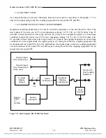
Page 148: ...ctions for the five RF modules that plug into it from the front of the chassis which are the TX Filter Balance Board Line Board Attenuator Board and Rx Filter Figure 7 14 shows the rear view of the mo...

Page 149: ...B1 5 External Amp Fail Relay NO TB1 6 External Amp Fail Relay NC TB1 7 Chassis Ground TB1 8 Earth Ground 7 9 2 GROUND CONNECTION AT TB1 8 At TB1 8 on the Mother Board Rear Panel a ground wire should b...

Page 150: ...Adapters MA 271 MA 278 8 2 CM4 Optical Interface Adapters 107455 201 301 401 501 8 3 PLC TT Module 105720 2 8 4 PLC TT Module Adapters 105740 2 to 5 105770 2 to 5 8 5 Teleprotection Transceiver 107830...

Page 151: ...Aux Trip Out 4 Aux Trip In 4 Bus Trip out 1 Trip out 2 Trip out 3 Trip Out 4 Trip In 1 Trip In 2 Trip In 3 Trip In 4 Alarm Trip Out 4 Trip In 4 Alarm Trip out 1 Trip out 2 Trip out 3 Trip Out 4 Trip...

Page 152: ...ot 10 while in drop insert applications the 9508D contains two CM4 Common Modules one in slot 10 and one in slot 1 8 1 1 CM4 OPERATIONAL FUNCTIONS The CM4 is the standard T1 E1 Common Module for the R...

Page 153: ...nal A jitter buffer is used to smooth out the timing jitter usually present on incoming signals The T1 E1 line output connection is made through a Module Adapter in 9508D chassis with electrical T1 E1...

Page 154: ...r Bus B This versatile bus capability enables simple configuration of a multiplexer as either terminal or drop insert Bus A B nomenclature is used to set channel modules to transmit and receive throug...

Page 155: ...channel module The RFL 9508D chassis provides 18 rear access Module Adapter slots one corresponding to each of the 18 front access module slots All 9508D Module Adapters have the same connector on th...

Page 156: ...e numbers in the item column of this table refers to the numbers in the boxes shown in Figure 8 5 9508D DIGITAL CHASSIS MAIN POWER SUPPLY MODULE CM4 COMMON MODULE IN SLOT 10 POWER 7 8 9 10 11 12 13 14...

Page 157: ...s closed four LED indicators are visible These LEDs are labeled POWER NORMAL ALERT and ALARM as shown in Figure 8 6 and indicate the operational status of the 9508D chassis at a glance Table 8 2 gives...

Page 158: ...on the ALERT and ALARM relays are on line and will activate in response to system fault conditions NOTE If the 9508D contains two power supply modules the ACO switches on both power supply modules mus...

Page 159: ...tam jacks Item Fig 8 5 Module Label Description 7 CM4 T1 OUT EQUIP Provides out of service test access to the CM4 s T1 output When in use this jack disconnects the CM4 s T1 transmitter from the T1 I O...

Page 160: ...ivity indicator consisting of three green LEDs RFL 9508D UCC RFL Electronics Inc ACTIVE ACTIVE When lit this CM4 is the active board BRD OK When lit this CM4 module is functional CONFIG When lit this...

Page 161: ...T1 mode Common module firmware revision Fcty When set returns Common Module to factory default setup Int ESF B8ZS ADDR Multiplexer address ddd A three digit number 001 to 500 Remote port serial parame...

Page 162: ...Name Function Description FTIM Fallback Timing FLoo Set fallback timing Loop FInt Set fallback timing to Internal FExt Set fallback timing to External FThru Set fallback timing to Through exit exit JB...

Page 163: ...flowed This may indicate that the receive signal contains excessive jitter RVU1 RcLs Receiver Carrier Loss When the Receiver Carrier Loss function is displayed the bi color ON OFF indicator will light...

Page 164: ...1 FTIM XsJt MAIN On Off Auto Main Stby BAUD 110 300 1200 PAR 2400 4800 9600 19 200 38 400 57 600 115 000 exit Univ Lock Spac Mark Even Odd exit SQEL PRSQ DISA 0 0m 0 66m 1 3m 2 0m 2 7m 3 3m 4 0m 4 6m...

Page 165: ...uously indicates the fallback timing mode which is now in effect The meaning of the LOOP indicator depends on the multiplexer type In terminal multiplexers the LOOP indicator indicates loop timing In...

Page 166: ...icates transmit status ON Transmission signal is normal It can be either data or all ones if the shelf is idle OFF No signal is being transmitted indicating a hardware failure LPBK Loopback indicator...

Page 167: ...ously indicates the fallback timing mode which is now in effect The meaning of the LOOP indicator depends on the multiplexer type In terminal multiplexers the LOOP indicator indicates loop timing In d...

Page 168: ...icates transmit status ON Transmission signal is normal It can be either data or all ones if the shelf is idle OFF No signal is being transmitted indicating a hardware failure LPBK Loopback indicator...

Page 169: ...T1 receiver input OFF No receive signal is detected BLINKING One of the following signals or conditions is detected View the BLNK group Paragraph 5 9 to determine which condition is causing the blinki...

Page 170: ...face adapters This section discusses CM4 electrical interface adapters CM4 Optical Interface adapters are discussed in paragraph 8 3 Electrical interface adapters are used to connect the 9508D electri...

Page 171: ...t n o t i c e Module Descriptions RFL 9508D Digital Section Pin Function 1 E1 IN 2 E1 IN 3 4 E1 OUT 5 E1 OUT RFL 9508D UCC RFL Electronics Inc 6 7 GND 8 GND Pin Function 1 TIMIN 2 TIMIN 3 4 5 TIMOUT 6...

Page 172: ...TEMS ARE INHERENTLY SAFE IN NORMAL OPERATION BECAUSE ALL RADIATION IS CONTAINED IN THE SYSTEM IT IS POSSIBLE DURING MAINTENANCE TO EXPOSE THE RADIATION BY REMOVING OR BREAKING THE FIBER STARING DIRECT...

Page 173: ...gital Section RFL 9508D UCC RFL Electronics Inc Pin Function 1 2 TXD_OUT 3 RXD_IN 4 5 GND 6 7 8 9 Pin Function 1 TIMIN 2 TIMIN 3 4 5 TIMOUT 6 TIMOUT Figure 8 10 Typical CM4 Optical Interface Adapter O...

Page 174: ...y Lower Limit Receiver Sensitivity Lower Limit With 3 dB Margin Typical Line Length 1300 nm SM LED OIA R CM4 RFL 9508D UCC RFL Electronics Inc 107455 201 1300 nm Singlemode 14dBm 17dBm 40 dBm 37 dBm 1...

Page 175: ...n operate point to point between two 9508D terminal nodes in a network The terminal nodes can be configured as point to point or drop and insert terminals and can be installed at different locations i...

Page 176: ...y the user but is set at the factory to 100 s ALARM TIMER This is a timer function which requires that an alarm condition exists for a certain length of time before an alarm output is generated The le...

Page 177: ...erature 20o C to 65o C Storage temperature 40o C to 75o C Humidity 95 40o C non condensing SWC FAST TRANSIENT ANSI C37 90 dielectric ANSI C37 90 1 SWC fast transient RFI SUSCEPTIBILITY ANSI C37 90 2 3...

Page 178: ...um operate time 10 ms OPERATING MODES Full duplex transmit and receive POWER CONSUMPTION 2 0 watts maximum DIMENSIONS Transfer Trip Module 2 Function I O Adapter Module 8 4 3 1 1 1 1 4 Functio n I O A...

Page 179: ...125V relay 105740 3 2 function 250V relay 105740 4 4 function 48 125V relay 105740 5 4 function 250V relay 105770 2 2 function 48 125V solid state 105770 3 2 function 250V solid state 105770 4 4 func...

Page 180: ...n a Typical 2 function Module Adapter b Typical 4 function Module Adapter 2TT I O 48 125V 105770 2 IN IN TRIP2 TRIP1 OUT OUT C NC NO ALARM 4TT I O 48 125V 105770 4 IN IN TRIP4 TRIP3 OUT OUT IN IN TRIP...

Page 181: ...17 18 NOTE 1 This cable must be installed when a second PLC TT I O is installed PLC TT I O B SEE NOTE 1 MAIN POWER SUPPLY REDUNDANT POWER SUPPLY CM 4 OPTIONAL PLC TT MODULE CM 4 MAIN TEST PANEL ANALOG...

Page 182: ...module performs the following functions Translates and converts the digital baseband source from the T1 E1 digital frame into the frequency range from 20 kHz to 500 kHz using Single Side Band modulat...

Page 183: ...e if the line quality is good enough to transmit at a higher bit rate or to make a fallback if the bit errors exceed a predetermined threshold line quality decreases 2 Translates and converts the Line...

Page 184: ...and 3249 symbols s with a 4KHz QAM spectrum bandwidth and 4800 5486 5600 6000 6400 and 6498 symbols s for an 8 KHz QAM spectrum bandwidth d Depending on the Power Line Conditions the following standar...

Page 185: ...M4 module the teleprotection Transceiver module or the Digital Transceiver module using a PC or laptop Through the Craft port a user can change or view the configuration of any channel cards in the lo...

Page 186: ...he PLC TT front panel or by using NMS or SOE The Test panel is only installed when a PLC TT module is installed The Test Panel has an eight conductor cable which plugs into JP1 of the PLC TT module Wh...

Page 187: ...types of power supplies that can be used with the 9508D Digital Chassis as shown in Table 8 16 The 9508D Digital Chassis can be powered with either one or two Power Supply modules The first power supp...

Page 188: ...TP9 TP10 15 Volt output Output circuit common 5Volt output 15 Volt output Output circuit common 15 Volt output 5 Volt output NA 15 Volt output 48Vdc output NA NA NA NA Input circuit common FET gate dr...

Page 189: ...chassis Some of the characteristics of these modules are listed in Table 8 18 A rear panel view of the 9547 18809 Power Supply Alarm I O module is shown in Figure 8 17 When a Main Shelf is equipped w...

Page 190: ...with 250Vdc power supplies 2000 PS ALARM I O 48 125 DC 9547 18804 Used in chassis equipped with 48 125 Vdc power supplies Used in chassis equipped with 48 125 Vdc power supplies and also provides swi...

Page 191: ...o allow modules to be plugged into the front and rear of the digital chassis The motherboard has a total of eighteen card slots as shown in Figure 5 2 but slots 8 and 16 are not used for modules Slot...

Page 192: ...s available for use with the RFL 9508D UCC Digital Power Line Carrier Multiplexing System as of the date this manual was printed o RFL VF 5XP Dual Channel Four Wire E M Voice Module o RFL PLC TT Trans...

Page 193: ...n u o u s p r o d u c t i mp r o v e me n t wer e s e r v et h er i g h t t oc h a n g ed e s i g n s a n ds p e c i c a t i o n s wi t h o u t n o t i c e Channel Modules This page intentionally left...

Page 194: ...o uses two 64 Kbps time slots The RFL VF 5XP provides high quality voice characteristics It allows E M signaling of Type I II III and V with front panel busy indicators It has extended range input and...

Page 195: ...s to status registers including board and firmware revision levels is also provided through NMS Signal Levels CH1 TLP transmit range 23 dBm to 10 dBm nominal 13 dBm peak TLP receive range 31 5 dBm to...

Page 196: ...35 volts Idle Open E Lead Output Busy Less than 35 ohms to ground Idle 42 to 60 volts or open Module Adapters MA 301 MA 301A MA 301B MA 322 or MA 324 Power Consumption 120 mA max from 5V supply 70 mA...

Page 197: ...xer manual for more information The following instructions are provided for installing RFL VF 5XP modules into existing systems If the module was included as part of a system installation was done at...

Page 198: ...onnections for a single VF 5XP module Audio and signaling connections are available at the terminal block No additional SWC or fast transient protection is provided on this I O Refer to Figure 4 for p...

Page 199: ...2007 6 973 334 3100 E M SIGNALING LEADS CHANNEL VF IN R T VF OUT R T SG E SB M 1 2 1 26 5 30 2 27 6 31 3 7 28 32 4 8 29 33 3 4 9 34 13 38 10 35 14 39 11 15 36 40 12 16 37 41 5 6 17 42 21 46 18 43 22...

Page 200: ...C H A N N E L 1 C H A N N E L 2 Figure 3 MA 301A SWC rated 4 wire Module Adapter SIGNAL TB AIN 1T 1 AIN 1R 2 AOUT 1T 3 AOUT 1R 4 M CH1 5 SB CH1 6 E CH1 7 SG CH1 8 AIN 2T 9 AIN 2R 10 AOUT 2T 11 AOUT 2R...

Page 201: ...g VF IN Channel 2 Ring 6 Not Used VF OUT Channel 2 Ring 7 SG Channel 2 SG Channel 2 8 SB Channel 2 SB Channel 2 26 Channel 1 Tip Channel 1 Tip 28 E Channel 1 E Channel 1 29 M Channel 1 M Channel 1 30...

Page 202: ...a guide 5 Refer to Figure 6 and Table 1 for the location of switches controls and indicators on the VF 5XP 6 Set DIP switches SW1 1 through SW1 6 for the desired remote access address For remote acces...

Page 203: ...er i g h t t oc h a n g ed e s i g n s a n ds p e c i c a t i o n s wi t h o u t n o t i c e 1 2 3 6 4 DS3 DS2 DS1 DS6 DS5 DS4 DS9 DS8 DS7 See Table 1 For LED functions 1 2 3 5 4 A A B B A A B B A A...

Page 204: ...near end configured for Remote Loopback RFL 9508 VF 5XP NEAR END TRANSMIT RECEIVE RFL 9508 VF 5XP FAR END TRANSMIT RECEIVE TERMINA L EQUIP MENT TERMINAL EQUIP MENT POWER LINE RFEQ RFEQ CM4 TRANSCEIVER...

Page 205: ...ead LED has two states Off Signaling is OFF or signaling is ON and M Lead input is inactive Green Signaling is ON and M Lead input is active 3 DS4 LED Channel 2 Enabled LED has three states Off CH2 Di...

Page 206: ...7 Jumper 8 J8 Jumper 9 J11 Jumper 10 J9 Jumper 11 J10 Jumper 12 J12 Jumper 13 J13 Jumper inserted toward front of board Sonalert Enabled Jumper inserted toward back of board Sonalert Disabled 14 J2 Us...

Page 207: ...ON OFF 7 OFF OFF OFF ON ON ON 8 OFF OFF ON OFF OFF OFF 9 OFF OFF ON OFF OFF ON 10 OFF OFF ON OFF ON OFF 11 OFF OFF ON OFF ON ON 12 OFF OFF ON ON OFF OFF 13 OFF OFF ON ON OFF ON 14 OFF OFF ON ON ON OFF...

Page 208: ...19 0 0 077 20 20 0 0 069 21 21 0 0 062 22 22 0 0 055 23 23 0 dBm dBm dBm Vrms 0 10 10 2 449 0 9 9 2 183 0 8 8 1 946 0 7 7 1 734 0 6 6 1 546 0 5 5 1 377 0 4 4 1 228 0 3 3 1 094 0 2 2 0 975 0 1 1 0 869...

Page 209: ...side of the VF 5XP it decodes the digital data into the appropriate analog voice frequency output referenced to 600 ohms The VF 5XP can be configured via NMS software All settings can be configured a...

Page 210: ...CEIVERS LEDs TRANS FORME R TRANS FORME R TRANS FORME R TRANS GAIN GAIN GAIN GAIN CODEC CODEC A D CONVERTER D A CONVERTER 4 ANALOG SECTION DIGITAL SECTION CH1 TX CH1 RX CH2 TX CH2 RX TIP RING TIP RING...

Page 211: ...ment Figure 9 Typical transmission only TO application using VF 5XP VF 5XP w signaling enabled CM VF 5XP w signaling enabled CM Powerline 9508 9508 Handset Handset Figure 10 Typical push to talk appli...

Page 212: ...open circuit on hook and ground off hook Type II Type II signaling is a four wire scheme normally encountered in electronic switching systems An on hook idle condition is indicated by open circuits on...

Page 213: ...P Type III Interface Battery Detector Ground Detector M M E E R P Trunk Circuit VF 5XP 48V SB SB SG SG 48V Ferrod Sensor 98 38 Ground Detector Ground Detector M M E E R P Trunk Circuit VF 5XP 48V 48V...

Page 214: ...nt Software version 10 5 or later Refer to the RFL 9508 Instruction Manual for information on using NMS To program the VF 5XP module go to the View or Change a Card window for the VF 5XP as shown in F...

Page 215: ...transmits in the B direction and receives from the A direction In a typical RFL9508 system this is set to TXA 5 Tx1 Level Adjust Sign The Tx1 Level can be set from 23dBm to 10dBm in 0 5dBm steps First...

Page 216: ...6 Rx2 Level Adjust Sign The Rx2 Level can be set from 31 5dBm to 10dBm in 0 5dBm steps First select the sign by clicking on the or then select the level as described in step 17 below 17 Rx2 Level Volu...

Page 217: ...ime any audio through channel 1 of the VF 5XP used for the service channel will be muted and audio through channel 2 of the VF 5XP is optionally muted with the MUTE CH2 IN SVC CHAN MODE setting When t...

Page 218: ...IM set or equivalent to the equipment input jack for the channel being tested Insert a 1004 kHz test tone at the TX level selected for that channel referenced to 600 ohms NOTE For the following steps...

Page 219: ...p o l i c yo f c o n t i n u o u s p r o d u c t i mp r o v e me n t wer e s e r v et h er i g h t t oc h a n g ed e s i g n s a n ds p e c i c a t i o n s wi t h o u t n o t i c e RFL VF 5XP RFL Elec...

Page 220: ...p o l i c yo f c o n t i n u o u s p r o d u c t i mp r o v e me n t wer e s e r v et h er i g h t t oc h a n g ed e s i g n s a n ds p e c i c a t i o n s wi t h o u t n o t i c e RFL VF 5XP RFL Elec...

Page 221: ...l system of any nature unless written permission is given by RFL Electronics Inc This publication has been compiled and checked for accuracy The information in this publication does not constitute a w...

Page 222: ...Directional Comparison Blocking in addition to two transfer trip functions These terminals can operate point to point between two RFL 9508 terminal nodes in a network These terminal nodes can be confi...

Page 223: ...ammable by the user but is set at the factory to 100 s ALARM TIME DELAY This timer function requires that an alarm condition exists for a certain length of time before an alarm output is generated The...

Page 224: ...37 90 1989 service conditions Operating temperature 20oC to 65oC Storage temperature 40oC to 75oC Humidity 95 40oC non condensing SWC FAST TRANSIENT ANSI C37 90 dielectric ANSI C37 90 1 SWC fast trans...

Page 225: ...t voltage Maximum operate time 1 A inductive 1 A resistive 280 Vdc 10 ms OPERATING MODES Full duplex transmit and receive POWER CONSUMPTION 2 0 watts maximum DIMENSIONS Transfer Trip Module 2 Function...

Page 226: ...its I O adapter module for shipping damage If you suspect damage to the module or its Module Adapter immediately contact RFL s Customer Service Department at the number shown at the bottom of this pa...

Page 227: ...LE 3 Switch SW3 Not Used 4 LED indicator red Lights when function 4 trip is received 5 LED indicator red Lights when function 3 trip is received 6 LED indicator red Lights when function 2 trip is rece...

Page 228: ...s e r v et h er i g h t t oc h a n g ed e s i g n s a n ds p e c i c a t i o n s wi t h o u t n o t i c e Figure 2 Rear panel view of typical 2 function RFL PLC TT Adapter Module Figure 3 Rear panel...

Page 229: ...jumpers in Figure 4 For 48V operation both jumpers must be in the 48V position For 125V operation both jumpers must be in the 125V position The 250V modules should have both jumpers in the 125V posit...

Page 230: ...wn in Table 3 The module address is usually set to the number of the physical slot in the shelf that the module will occupy it can be set to any number from 1 to 31 that is not already being used by a...

Page 231: ...N 3 DOWN DOWN DOWN UP UP 4 DOWN DOWN UP DOWN DOWN 5 DOWN DOWN UP DOWN UP 6 DOWN DOWN UP UP DOWN 7 DOWN DOWN UP UP UP 8 DOWN UP DOWN DOWN DOWN 9 DOWN UP DOWN DOWN UP 10 DOWN UP DOWN UP DOWN 11 DOWN UP...

Page 232: ...ld programmable gate array and its associated circuits handles all T1 E1 communication and trip I O The SCB FPGA connects the processor with the SCB of the 9508 Miscellaneous other circuits are presen...

Page 233: ...n u o u s p r o d u c t i mp r o v e me n t wer e s e r v et h er i g h t t oc h a n g ed e s i g n s a n ds p e c i c a t i o n s wi t h o u t n o t i c e Figure 5 Transfer Trip module block diagram...

Page 234: ...are sized to allow a safe level of current to be drawn from the keying input The zener diode and resistors prevent any voltage less than half the nominal keying voltage from causing an input The optoi...

Page 235: ...e To set these bits in NMS one should select output polarity for output 1 or 2 and change it appropriately ALERTS AND ALARMS If there is a loss of signal or if the disable switch is down the transfer...

Page 236: ...agement Software version 10 5 or later Refer to the IMUX 2000 Instruction Manual for information on using NMS To program the PLC TT module go to the PLC TT View or Change a Card Window as shown in Fig...

Page 237: ...teps Output 1 Polarity Output 2 Polarity Output 3 Polarity Output 4 Polarity Inverted Not Inverted Output 1 Unblock Enable Output 2 Unblock Enable Output 3 Unblock Enable Output 4 Unblock Enable Enabl...

Page 238: ...3 Command Sent 4 Active Inactive Command Received 1 Command Received 2 Command Received 3 Command Received 4 Active Inactive PLC Channel Status Good Channel Transceiver Hardware Alarm PLC Channel Fai...

Page 239: ...age to be used in service An indicator capable of detecting operation of the trip outputs TEST PROCEDURE Once the module has been installed in an operating RFL 9508 system the disable switch can be pl...

Page 240: ...i c yo f c o n t i n u o u s p r o d u c t i mp r o v e me n t wer e s e r v et h er i g h t t oc h a n g ed e s i g n s a n ds p e c i c a t i o n s wi t h o u t n o t i c e RFL 9508 PLC TT RFL Elec...

Page 241: ...re unless written permission is given by RFL Electronics Inc This publication has been compiled and checked for accuracy The information in this publication does not constitute a warranty of performan...

Page 242: ...GENERATOR 4 20 REMOTE CHANNEL BOXES 4 20 CONNECTING PC TO NETWORK 4 5 D DATA TRANSMISSION CHARACTERISTICS 8 35 DIGITAL CHASSIS CABLING 5 7 FRONT PANEL SWITCHES INDICATORS JACKS 8 7 LOOP INT AND EXT I...

Page 243: ...RE 4 1 INSTALLING 4 2 STARTING 4 11 SYSTEM REQUIREMENTS 4 1 UN INSTALLING 4 4 USING 4 11 P P0WER AMP BOARD DIP SWITCH SETTINGS 5 31 PERFORMANCE RX FILTER 2 10 PERMORMANCE TX FILTER 2 10 PLACEMENT AND...

Reviews: