


No TV but PC is present
1. Check if HSYNC and VSYNC are present at PIN 3 of 7071 and 7015.
2. If they are present, check RGB output.
3. If there is no RGB output, the IC TDA120xx can be failed.
Comb Filter not working
1. Check the option bit 5 in SAM.
2. Check NVM setting. Address 1229 is 0000.
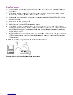
Power Supply
Check fuses
This power supply contains three fuses. One is near the mains inlet (marked on the board as
1102) and two other are near the output connectors (marked 1610 and 1660).
1. Check with power supply in off state by means of ohmic measurement.
2. Fuse 1102 may open in case of severe lightning strikes and/or failures in the power supply.
Despite the fact, that this fuse is mounted in a fuse holder and the marking text on the
board, it is not meant to be field replaceable.
3. Fuses 1610 and 1660 may open in case a severe overload of the 12 V outputs.
Replacement of the power supply is needed, but not before the cause of the overload
conditions is resolved.
Standby mode
1. Apply a 12 ohm load resistor of sufficient power rating to all outputs (+3 V3, +12 VAL, +12
VL and +24 V). Connect the STBY pin to GND.
2. Over an input voltage range of 90 V_ac to 264 V_ac only the +3 V3 output shall be up and
within regulation (±5%). The voltage on the POWER DOWN pin shall be < 0.3 V at an input
voltage below 160 V_ac, and 3.3 V ±10% at an input voltage higher than 240 V_ac.
Normal mode:
1. Apply a 12 ohm load resistor of sufficient power rating to all outputs (+3 V3, +12 VAL, +12
VL and +24 V). Connect the STBY pin to the +3 V3 output.
2. Over an input voltage range of 90 V _ac to 264 V_ac all outputs shall be up and within
regulation (±5%). The voltage on the POWER DOWN pin shall be 3.3 V ±10% over the
entire input voltage range. Additionally, the voltage on the big capacitor mounted flat on the
PCB shall be 400 V ±10%.
Summary of Contents for 26FW5220
Page 1: ......
Page 5: ......
Page 39: ...SAM Menu Figure E14490 054 SAM Menu nieuw nummer ...
Page 45: ...All Models 7670 Chassis Overview ...
Page 46: ...All Models 7670 Power Supply A1 ...
Page 47: ...All Models 7670 Hercules A2 ...
Page 48: ...All Models 7670 Histogram A3 ...
Page 49: ...All Models 7670 Audio Amplifier A5 ...
Page 50: ...All Models 7670 TV Supply A6 ...
Page 51: ...All Models 7670 Scaler A7 ...
Page 52: ...All Models 7670 Scaler Interface A9 ...
Page 53: ...All Models 7670 SDRAM A10 ...
Page 54: ...All Models 7670 Flash Control A11 ...
Page 55: ...All Models 7670 HDMI A12 ...
Page 56: ...All Models 7670 PCHD MUX A13 ...
Page 57: ...All Models 7670 Supply A14 ...
Page 58: ...All Models 7670 3D Comb Filter CB ...
Page 59: ...All Models 7670 Side IO and LKB Panel D ...
Page 60: ...All Models 7670 Cinch 17 H1 ...
Page 61: ...All Models 7670 PCHD IO 17 H2 ...
Page 62: ...All Models 7670 Rear IO Cinch 23 26 H1 ...
Page 63: ...All Models 7670 PCHD IO 23 26 H2 ...
Page 64: ...All Models 7670 Front IR LED Panel J ...
Page 65: ...All Models 7670 EPLD Control PP1 ...
Page 66: ...All Models 7670 LVDS In PP2 ...
Page 67: ...All Models 7670 EPLD I O PP3 ...
Page 68: ...All Models 7670 Power Supply PP4 ...
Page 69: ...All Models 7670 Layout Tv Scaler Board Overview Top Side ...
Page 70: ...All Models 7670 Layout Tv Scaler Board Overview Bottom Side ...
Page 71: ...All Models 7670 Layout 3D Comb Filter Top Side ...
Page 72: ...All Models 7670 Layout 3D Comb Filter Bottom Side ...
Page 73: ...All Models 7670 Layout Side IO and LKB Panel Top Side ...
Page 74: ...All Models 7670 Layout Side IO and LKB Panel Bottom Side ...
Page 75: ...All Models 7670 Layout Rear IO Panel 17 Top Side ...
Page 76: ...All Models 7670 Layout Rear IO Panel 17 Bottom Side ...
Page 77: ...All Models 7670 Layout Rear IO Panel 23 26 Top Side ...
Page 78: ...All Models 7670 Layout Rear IO Panel 23 26 Bottom Side ...
Page 79: ...All Models 7670 Layout Front IR LED Panel Top Side ...
Page 80: ...All Models 7670 Layout Front IR LED Panel Bottom Side ...
Page 81: ...All Models 7670 Layout Pixel Plus Panel Top Side ...
Page 82: ...All Models 7670 Layout Pixel Plus Panel Bottom Side ...
Page 83: ...All Models 7670 Testpoint Overview TV Scaler Board Bottom Side ...
Page 84: ...All Models 7670 Testpoint Overview TV Scaler Board Top Side ...
Page 85: ...All Models 7670 Wiring Diagram ...
Page 86: ...All Models 7670 Block Diagram Tuner and IF Video ...
Page 87: ...All Models 7670 Block Diagram Scaler ...
Page 88: ...All Models 7670 I2C IC Overview ...
Page 89: ...All Models 7670 Supply Voltage Overview ...
Page 109: ...Diagram A7 Type GM1501 IC7401 Figure Internal Block Diagram and Pin Configuration ...
Page 110: ...Diagram A12 Type S9993CT IC7808 Figure Internal Block Diagram ...


