


l
SCL.
This is the clock wire of the two-wire single master bi-directional I2C bus.
l
SDA.
This is the data wire of the two-wire single master bi-directional I2C bus.
l
STANDBY.
The Hercules generates this signal. This can enable the power supply
in normal operation and disable it during Standby. It is of logic “high” (3.3 V) under
normal operation and “low” (0 V) during Standby.
l
IR.
This input pin is connected to an RC5 remote control receiver.
l
SEL-IF.
This is an output pin to switch the Video SAW filter between M system and
other systems.
n
0: NTSC M (default)
n
1: PAL B/G, DK, I, L
l
NVM_WP.
The global protection line is used to enable and disable write protection
to the NVM. When write to the NVM is required, pin 7 of the NVM must be pulled to
logic '0' first (via Write_Protect of the micro-controller pin) before a write is
performed. Otherwise pin 7 of NVM must always be at logic “1”
n
0: Disabled
n
1: Enabled (default)
l
SOUND_ENABLE.
This pin is use to MUTE the audio amplifier. It is configured as
push pull.
l
STATUS_1.
This signal is used to read the status of the SCART 1 input.
l
STATUS_2.
This signal is used to read the status of the SCART 2 input.
l
HERC_RESET.
This pin is use to switch the +1.8V supply.
l
POWER_DOWN. The power supply generates this signal. Logic “high” (3.3 V)
under normal operation of the TV and goes “low” (0 V) when the Mains input
voltage supply goes below 70 V_ac.
122 P2.4/ PWM3 STANDBY P2.4
123 P2.5/ PWM4 (for future use) -
126 P1.2/ INT2 (for future use) -
127 P1.4/ RX HERC_RESET -
128 P1.5/ TX POWER_DOWN P1.5
l
Keyboard. Following are the Keyboard functions and the step values (8 bit) for it.
Table: Local keyboard values
l
TV_IRQ.
This signal is the interrupt from the Scaler IC.
l
TV_SC_COM.
This signal is used for the communication with the Scaler IC.
l
EXT_MUTE.
This signal is used to reduce the Switch-off plop.
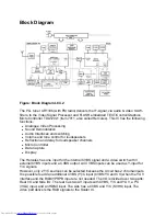
Summary of Contents for 26FW5220
Page 1: ......
Page 5: ......
Page 39: ...SAM Menu Figure E14490 054 SAM Menu nieuw nummer ...
Page 45: ...All Models 7670 Chassis Overview ...
Page 46: ...All Models 7670 Power Supply A1 ...
Page 47: ...All Models 7670 Hercules A2 ...
Page 48: ...All Models 7670 Histogram A3 ...
Page 49: ...All Models 7670 Audio Amplifier A5 ...
Page 50: ...All Models 7670 TV Supply A6 ...
Page 51: ...All Models 7670 Scaler A7 ...
Page 52: ...All Models 7670 Scaler Interface A9 ...
Page 53: ...All Models 7670 SDRAM A10 ...
Page 54: ...All Models 7670 Flash Control A11 ...
Page 55: ...All Models 7670 HDMI A12 ...
Page 56: ...All Models 7670 PCHD MUX A13 ...
Page 57: ...All Models 7670 Supply A14 ...
Page 58: ...All Models 7670 3D Comb Filter CB ...
Page 59: ...All Models 7670 Side IO and LKB Panel D ...
Page 60: ...All Models 7670 Cinch 17 H1 ...
Page 61: ...All Models 7670 PCHD IO 17 H2 ...
Page 62: ...All Models 7670 Rear IO Cinch 23 26 H1 ...
Page 63: ...All Models 7670 PCHD IO 23 26 H2 ...
Page 64: ...All Models 7670 Front IR LED Panel J ...
Page 65: ...All Models 7670 EPLD Control PP1 ...
Page 66: ...All Models 7670 LVDS In PP2 ...
Page 67: ...All Models 7670 EPLD I O PP3 ...
Page 68: ...All Models 7670 Power Supply PP4 ...
Page 69: ...All Models 7670 Layout Tv Scaler Board Overview Top Side ...
Page 70: ...All Models 7670 Layout Tv Scaler Board Overview Bottom Side ...
Page 71: ...All Models 7670 Layout 3D Comb Filter Top Side ...
Page 72: ...All Models 7670 Layout 3D Comb Filter Bottom Side ...
Page 73: ...All Models 7670 Layout Side IO and LKB Panel Top Side ...
Page 74: ...All Models 7670 Layout Side IO and LKB Panel Bottom Side ...
Page 75: ...All Models 7670 Layout Rear IO Panel 17 Top Side ...
Page 76: ...All Models 7670 Layout Rear IO Panel 17 Bottom Side ...
Page 77: ...All Models 7670 Layout Rear IO Panel 23 26 Top Side ...
Page 78: ...All Models 7670 Layout Rear IO Panel 23 26 Bottom Side ...
Page 79: ...All Models 7670 Layout Front IR LED Panel Top Side ...
Page 80: ...All Models 7670 Layout Front IR LED Panel Bottom Side ...
Page 81: ...All Models 7670 Layout Pixel Plus Panel Top Side ...
Page 82: ...All Models 7670 Layout Pixel Plus Panel Bottom Side ...
Page 83: ...All Models 7670 Testpoint Overview TV Scaler Board Bottom Side ...
Page 84: ...All Models 7670 Testpoint Overview TV Scaler Board Top Side ...
Page 85: ...All Models 7670 Wiring Diagram ...
Page 86: ...All Models 7670 Block Diagram Tuner and IF Video ...
Page 87: ...All Models 7670 Block Diagram Scaler ...
Page 88: ...All Models 7670 I2C IC Overview ...
Page 89: ...All Models 7670 Supply Voltage Overview ...
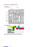
Page 109: ...Diagram A7 Type GM1501 IC7401 Figure Internal Block Diagram and Pin Configuration ...
Page 110: ...Diagram A12 Type S9993CT IC7808 Figure Internal Block Diagram ...


