


SMPS
Switch Mode Power Supply
SND
SouND
SNDL-SC1-IN
Sound left SCART1 in
SNDL-SC1-OUT
Sound left SCART1 out
SNDL-SC2-IN
Sound left SCART2 in
SNDL-SC2-OUT
Sound left SCART2 out
SNDR-SC1-IN
Sound right SCART1 in
SNDR-SC1-OUT
Sound right SCART1 out
SNDR-SC2-IN
Sound right SCART2 out
SNDR-SC2-OUT
Sound right SCART2 out
SNDS-VL-OUT
Surround sound left variable level out
SNDS-VR-OUT
Surround sound right variable level out
SOPS
Self Oscillating Power Supply
S/PDIF
Sony Philips Digital InterFace
SRAM
Static RAM
STBY
STandBY
SVHS
Super Video Home System
SW
SubWoofer / SoftWare
THD
Total Harmonic Distortion
TXT
TeleteXT
UP
Microprocessor
VA
Vertical Acquisition
VL
Variable Level out: processed audio output toward external
amplifier
VCR
Video Cassette Recorder
VGA
Video Graphics Array
WD
Watch Dog
WYSIWYR
What You See Is What You Record: record selection that
follows main picture and sound
XTAL
Quartz crystal
YpbPr
Component video (Y= Luminance, Pb/Pr= Colour difference
signals)
Y/C
Luminance (Y) and Chrominance (C) signal
Y-OUT
Luminance-signal
YUV
Component video
Summary of Contents for 26FW5220
Page 1: ......
Page 5: ......
Page 39: ...SAM Menu Figure E14490 054 SAM Menu nieuw nummer ...
Page 45: ...All Models 7670 Chassis Overview ...
Page 46: ...All Models 7670 Power Supply A1 ...
Page 47: ...All Models 7670 Hercules A2 ...
Page 48: ...All Models 7670 Histogram A3 ...
Page 49: ...All Models 7670 Audio Amplifier A5 ...
Page 50: ...All Models 7670 TV Supply A6 ...
Page 51: ...All Models 7670 Scaler A7 ...
Page 52: ...All Models 7670 Scaler Interface A9 ...
Page 53: ...All Models 7670 SDRAM A10 ...
Page 54: ...All Models 7670 Flash Control A11 ...
Page 55: ...All Models 7670 HDMI A12 ...
Page 56: ...All Models 7670 PCHD MUX A13 ...
Page 57: ...All Models 7670 Supply A14 ...
Page 58: ...All Models 7670 3D Comb Filter CB ...
Page 59: ...All Models 7670 Side IO and LKB Panel D ...
Page 60: ...All Models 7670 Cinch 17 H1 ...
Page 61: ...All Models 7670 PCHD IO 17 H2 ...
Page 62: ...All Models 7670 Rear IO Cinch 23 26 H1 ...
Page 63: ...All Models 7670 PCHD IO 23 26 H2 ...
Page 64: ...All Models 7670 Front IR LED Panel J ...
Page 65: ...All Models 7670 EPLD Control PP1 ...
Page 66: ...All Models 7670 LVDS In PP2 ...
Page 67: ...All Models 7670 EPLD I O PP3 ...
Page 68: ...All Models 7670 Power Supply PP4 ...
Page 69: ...All Models 7670 Layout Tv Scaler Board Overview Top Side ...
Page 70: ...All Models 7670 Layout Tv Scaler Board Overview Bottom Side ...
Page 71: ...All Models 7670 Layout 3D Comb Filter Top Side ...
Page 72: ...All Models 7670 Layout 3D Comb Filter Bottom Side ...
Page 73: ...All Models 7670 Layout Side IO and LKB Panel Top Side ...
Page 74: ...All Models 7670 Layout Side IO and LKB Panel Bottom Side ...
Page 75: ...All Models 7670 Layout Rear IO Panel 17 Top Side ...
Page 76: ...All Models 7670 Layout Rear IO Panel 17 Bottom Side ...
Page 77: ...All Models 7670 Layout Rear IO Panel 23 26 Top Side ...
Page 78: ...All Models 7670 Layout Rear IO Panel 23 26 Bottom Side ...
Page 79: ...All Models 7670 Layout Front IR LED Panel Top Side ...
Page 80: ...All Models 7670 Layout Front IR LED Panel Bottom Side ...
Page 81: ...All Models 7670 Layout Pixel Plus Panel Top Side ...
Page 82: ...All Models 7670 Layout Pixel Plus Panel Bottom Side ...
Page 83: ...All Models 7670 Testpoint Overview TV Scaler Board Bottom Side ...
Page 84: ...All Models 7670 Testpoint Overview TV Scaler Board Top Side ...
Page 85: ...All Models 7670 Wiring Diagram ...
Page 86: ...All Models 7670 Block Diagram Tuner and IF Video ...
Page 87: ...All Models 7670 Block Diagram Scaler ...
Page 88: ...All Models 7670 I2C IC Overview ...
Page 89: ...All Models 7670 Supply Voltage Overview ...
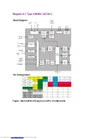
Page 109: ...Diagram A7 Type GM1501 IC7401 Figure Internal Block Diagram and Pin Configuration ...
Page 110: ...Diagram A12 Type S9993CT IC7808 Figure Internal Block Diagram ...


