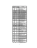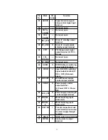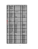
Pin
No.
Mark
I/O
Division
Function
30
PWM
I
PWM signal input terminal
(H: Output TR ON)
31
GND
—
GND terminal
32
FIL
O
Spindle motor position
detection comparator filter
output terminal
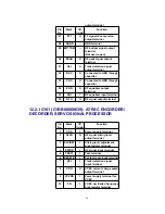
33
COMIN
I
Spindle motor position
detection comparator filter
input terminal
34
VCOIN
I
VCO control voltage input
terminal
(Connected to GND
through capacitor)
35
VCO
—
VCO oscillation output
terminal
(Connected to GND
through capacitor)
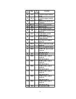
36
RMAX
—
VCO highest frequency
setting input terminal
(Connected to GND
through resistor)
37
IN2R
I
H bridge (2) logic reverse
input terminal
38
IN2F
I
H bridge (2) logic forward
input terminal
39
MUTE
I
H bridge 1,2 and 3-phase
sled mute input terminal
40
VS2
I
H bridge (2) motor power
supply input terminal
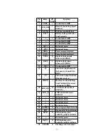
41
OUT2F
O
H bridge (2) forward output
terminal
42
OUT2R
O
H bridge (2) reverse output
terminal
43
PGND1
—
GND terminal
44
OUT1R
O
H bridge (1) reverse output
terminal
45
OUT1F
O
H bridge (1) forward output
terminal
46
VS1
I
H bridge (1) motor power
supply input terminal
47
S/S
I
Spindle motor block start/
stop input terminal (H:
Start)
58
Summary of Contents for SJ-MJ50GH
Page 5: ...3 Operating Instructions 4 Handling Precautions for MD Mechanism Optical 5 ...
Page 10: ... Check the P C B as shown below 10 ...
Page 11: ...5 2 Replacement for the disc cover ass y 11 ...
Page 12: ...5 3 Replacement for the side cabinet ass y Follow the Step 1 Step 3 of item 5 1 12 ...
Page 13: ...13 ...
Page 15: ...15 ...
Page 17: ...17 ...
Page 18: ...5 6 Replacement for the traverse motor Follow the Step 1 Step 3 of item 5 1 18 ...
Page 19: ...19 ...
Page 20: ...20 ...
Page 22: ...22 ...
Page 23: ...23 ...
Page 24: ...24 ...
Page 25: ...25 ...
Page 35: ...35 ...
Page 36: ...36 ...
Page 37: ...37 ...
Page 38: ...38 ...
Page 39: ...39 ...
Page 40: ...40 ...
Page 41: ...41 ...
Page 42: ...8 Schematic Diagram Notes 8 1 Type Illustration of IC s Transistors and Diodes 42 ...
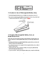
Page 53: ...29 CHARGE O Recharge control output terminal 53 ...


