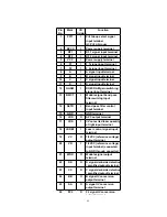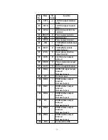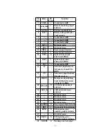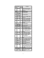
Pin
No.
Mark
I/O
Division
Function
53
SHOCK
I
Signal detection signal/
sleep control signal input
terminal
54
—
—
Not used, open
55
DATA_
FLASH
—
Not used, open
56
CLK_
FLASH
—
Not used, open
57 DRV_STBY O
Driver IC standby output
terminal
58 SP_STBY
O
Driver IC circuit spindle
standby output terminal
59
PPIT
O
Pit/ Group select signal
output terminal (H: Pit/ L:
Group)
60
LSI_
STATUS
—
Not used, open
61 ST_READ
—
Not used, open
62
GHSW
O
ROM/ RAM gain switching
signal output terminal
63
LDON
—
Laser ON/ OFF switching
signal output terminal (H:
ON/ L: OFF) (Not used,
open)
64 RFCONT
O
RF AMP power supply
control output terminal
65
P.CONT
O
Power supply control
output terminal
(H: Power OFF/ L: Power
ON)
66 MOD_CNT
O
Power supply switching IC
control output terminal
67
MODEL
1
I
Model switching input
terminal (1)
68
MODEL
2
I
Model switching input
terminal (2)
69 DOCTOR
I
Process inspection mode
input terminal (Connected
to power supply through
resistor)
70
HOLD
I
HOLD switch input terminal
71
MUTEA
O
Analog mute A output
terminal
55
Summary of Contents for SJ-MJ50GH
Page 5: ...3 Operating Instructions 4 Handling Precautions for MD Mechanism Optical 5 ...
Page 10: ... Check the P C B as shown below 10 ...
Page 11: ...5 2 Replacement for the disc cover ass y 11 ...
Page 12: ...5 3 Replacement for the side cabinet ass y Follow the Step 1 Step 3 of item 5 1 12 ...
Page 13: ...13 ...
Page 15: ...15 ...
Page 17: ...17 ...
Page 18: ...5 6 Replacement for the traverse motor Follow the Step 1 Step 3 of item 5 1 18 ...
Page 19: ...19 ...
Page 20: ...20 ...
Page 22: ...22 ...
Page 23: ...23 ...
Page 24: ...24 ...
Page 25: ...25 ...
Page 35: ...35 ...
Page 36: ...36 ...
Page 37: ...37 ...
Page 38: ...38 ...
Page 39: ...39 ...
Page 40: ...40 ...
Page 41: ...41 ...
Page 42: ...8 Schematic Diagram Notes 8 1 Type Illustration of IC s Transistors and Diodes 42 ...
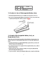
Page 53: ...29 CHARGE O Recharge control output terminal 53 ...

