


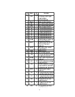
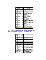


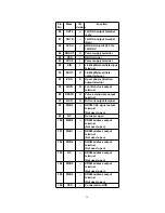


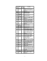


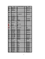


Pin
No.
Mark
I/O
Division
Function
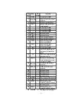
86
OUTL
—
1bit DAC output terminal
(Lch)
87
OUTR
—
1bit DAC output terminal
(Rch)
88
AVSS
—
GND terminal of LPF for
1bit DAC
89
DDOUT
O
Power supply terminal
90
VSS
—
GND terminal
91
VCC2
I
Power supply terminal
92
XIN
I
16.9344MHz oscillate input
terminal
93
XOUT
O
16.9344MHz oscillate
output terminal
94
ENH
O
De-emphasis direction
output terminal
95
LRCO
O
Lch/ Rch clock output
terminal
96
DDATA
O
Voice extend data output
terminal
97
BCO
O
Bit clock output terminal
98
MAD9
—
DRAM CAS signal output
terminal
(Not used, open)
99
NC
—
Not used, open
100
MAD8
—
DRAM address output
terminal
(Not used, open)
101
MAD7
—
DRAM address output
terminal
(Not used, open)
102
MAD6
—
DRAM address output
terminal
(Not used, open)
103
NC
—
DRAM address output
terminal
(Not used, open)
104
MAD5
—
DRAM address output
terminal
(Not used, open)
105
MAD4
—
DRAM address output
terminal
(Not used, open)
106
VSS
—
Connected to GND
50
Summary of Contents for SJ-MJ50GH
Page 5: ...3 Operating Instructions 4 Handling Precautions for MD Mechanism Optical 5 ...
Page 10: ... Check the P C B as shown below 10 ...
Page 11: ...5 2 Replacement for the disc cover ass y 11 ...
Page 12: ...5 3 Replacement for the side cabinet ass y Follow the Step 1 Step 3 of item 5 1 12 ...
Page 13: ...13 ...
Page 15: ...15 ...
Page 17: ...17 ...
Page 18: ...5 6 Replacement for the traverse motor Follow the Step 1 Step 3 of item 5 1 18 ...
Page 19: ...19 ...
Page 20: ...20 ...
Page 22: ...22 ...
Page 23: ...23 ...
Page 24: ...24 ...
Page 25: ...25 ...
Page 35: ...35 ...
Page 36: ...36 ...
Page 37: ...37 ...
Page 38: ...38 ...
Page 39: ...39 ...
Page 40: ...40 ...
Page 41: ...41 ...
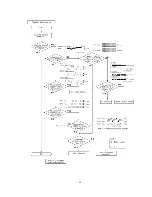
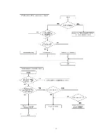
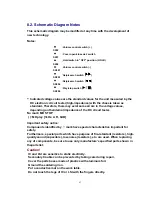
Page 42: ...8 Schematic Diagram Notes 8 1 Type Illustration of IC s Transistors and Diodes 42 ...
Page 53: ...29 CHARGE O Recharge control output terminal 53 ...