11 CIRCUIT DESCRIPTION
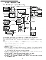
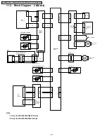
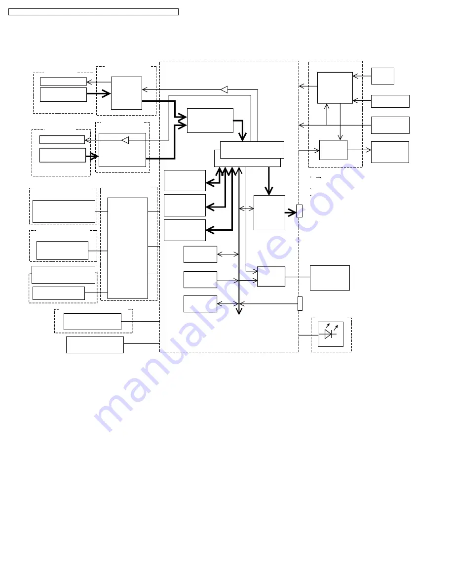
11.1. Block Diagram - 1 (Image Processing)
" " mentions image processing flow
from CIS to PC.
LED Driver &
Relay Circuit
Starting Position Sensor
Waiting Sensor
Imprinter
Ending Sensor
Paper Detector
Relay
Circuit
Image Sensor
Power Switch
Door Swirch
Paper Feed
Motor
AC Inlet
Conveyor
Motor
CPU
ROM
SRAM
Gate Array
IC1003 (*
1
IC1004,
IC1005, IC1006)
CN1004, CN1005
IC1505, IC1506
(*
1
IC1508, IC1509)
IC1510 (*
1
IC1511)
IC1501
IC1030
IC1035
IC1040
IC1041
(*
1
IC1502)
(*
1
IC1504, IC1507)
A/D Conv
SCSI
Controller
LED Source
Image Sensor
LED Source
Motor
Driver
Line Buffer
Memory
Shading Memory
SCSI Connector
Dip Switch
Motor
Driver
DC Power
Note:
SDRAM
Relay Circuit
+3.3V, +5V,
+12V, +24V
CIS (Front)
CIS (Back)
RELAY (FRONT)
Board (1/2)
RELAY (FRONT)
Board (2/2)
RELAY (BACK)
Board
STARTING POSTION
SENSOR Board
WAITING SENSOR
Board
ENDING SENSOR Board
LED Board
Option
(Only for KV-S2045C/
SU245C Series)
CONTROL Board
POWER Board
(
*1
....): Only for KV-S2045C/SU245C Series
(
*2
....): Only for KV-S2025C/S2045C Series
*
2
*
2
As a scanning device, this product adopts color CIS (Contact Image Sensor) for each scanning side independently.
The color CIS has Red, Green, and Blue LEDs. Changing the three colors enables it to scan color data.
Scanned data (Analogue) from the color CIS is transmitted to CONTROL Board via RELAY (FRONT) Board and RELAY (BACK)
Board.
The digital data, converted from analogue by A/D Conv. on the CONTROL Board, is processed according to the following protocol.
Note
·
A/D Conv. for KV-S2045C/SU245C Series: IC1003 to IC1006
·
A/D Conv. for KV-S2025C/SU225C Series: IC1003
1. In Case of KV-S2045C Series
a. Based on white standard data memorized in Shading Memory (IC1505, IC1506, IC1508, IC1509) in advance, Gate Arrays
(IC1501, IC1502) process the data from the A/D Conv. to do shading correction for each side independently. (IC1501: For
front side, IC1502: For back side)
After that, the Gate Arrays process Gamma transformation with the shading data.
b. The gamma data is arranged to each line data, and is memorized in Line Buffer Memory (IC1504, IC1507: Mounted only
for KV-S2045C Series) by the Gate Arrays.
c. The Gate Arrays process dpi transformation with the line data read from the Line Buffer Memory.
After finishing this process, the transformed data is written in SDRAM (IC1510, IC1511).
d. The Gate Arrays process MTF correction with the dpi data read from the SDRAM. And after that, the Gate Arrays write the
MTF data in the SDRAM, again.
80
KV-S2025C Series / KV-SU225C Series / KV-S2045C Series / KV-SU245C Series
Summary of Contents for KV-S2025C
Page 96: ...96 KV S2025C Series KV SU225C Series KV S2045C Series KV SU245C Series ...
Page 114: ...KV S2025C Series KV SU225C Series KV S2045C Series KV SU245C Series 114 ...
Page 116: ...14 1 Exterior 116 KV S2025C Series KV SU225C Series KV S2045C Series KV SU245C Series ...
Page 118: ...14 2 Chassis and Base 118 KV S2025C Series KV SU225C Series KV S2045C Series KV SU245C Series ...
Page 120: ...14 3 Hopper Unit 120 KV S2025C Series KV SU225C Series KV S2045C Series KV SU245C Series ...
Page 122: ...14 4 Power Unit 122 KV S2025C Series KV SU225C Series KV S2045C Series KV SU245C Series ...

