VEGA
Issue 1
Section 8
MCUK991001G8
Revision 0
– 32 –
Technical Guide
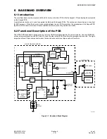
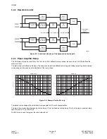
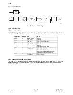
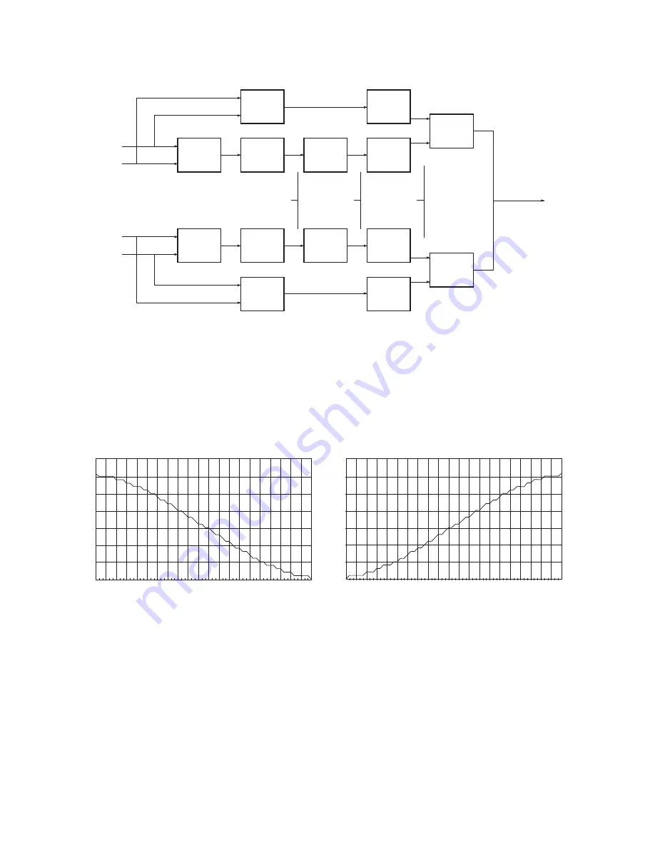
8.2.2 Downlink I and Q
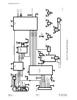
Figure 8.3: Functional structure of the baseband downlink path
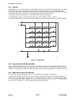
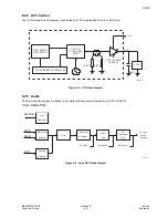
8.2.3 Power Amplifier Ramp
The PA Ramp is formed by two D/As. The first, a 5 bit D/A, defines the ramp shape; the second, an 8 bit D/A, defines the
maximum level.
The ramp shape is defined by 64 steps. The shape can be defined differently for rising and falling ramps. Typically a raised
cosine shape will be used as a starting basis of the ramp shape.
Figure 8.4: Example for the PA ramp
The raised cosine shape will be modified to compensate for RF circuit characteristics.
The ramp time is selectable between each step being 1/16 of a bit and each step being 1/8 of a bit giving a maximum ramp
time of either 14.77 µs or 29.53 µs.
An 8 bit value is used to program the ramp output level.
fs3=270.8 kHz
fs2=1.08 MHz
fs1=6.5 MHz
DLIP
DLIN
DLQP
DLQN
Antialiasing
Filter
Sigma_Delta
Modulator
SINC
Filter
To baseband
serial
interface
FIR
Filter
SUB
Offset
Calibration
SUB
Offset
Register
Antialiasing
Filter
Sigma_Delta
Modulator
SINC
Filter
FIR
Filter
Offset
Calibration
Offset
Register
10090-1
63
Step
0.00
5.00
10.00
15.00
20.00
25.00
30.00
35.00
0
3
6
9
12
15
18
21
24
27
30
33
36
39
42
45
48
51
54
57
60
5bit
D/A
Value
Ramp Up
0.00
5.00
10.00
15.00
20.00
25.00
30.00
35.00
0
3
6
9
12
15
18
21
24
27
30
33
36
39
42
45
48
51
54
57
60
5bit
D/A
Value
63
Step
Ramp Down
10091-1


