


BASEBAND OVERVIEW
MCUK991001G8
Section 6
Issue 1
Technical Guide
– 19 –
Revision 0
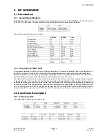
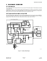
6 BASEBAND OVERVIEW
6.1 Introduction
The main Baseband circuitry is located with the RF circuits on the Main PCB, while the keypad, LCD and backlights are located
on the Keypad PCB.
A metallised plastic chassis is used to separate the Main and the Keypad PCBs. The continuous chassis design is important
for EMC purposes. When the chassis is sandwiched between the two PCB assemblies, the groundplane of the Keypad PCB
together with the chassis forms an effective shielded enclosure, preventing spurious emissions.
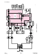
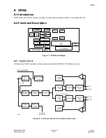
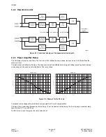
6.2 Functional Description of the PCB
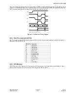
The GD30/GD50 baseband is based around a two-chip GSM chipset developed by Texas Instruments. One chip (GEMINI)
carries out signal processing with DSP and CPU, and the other chip (VEGA3) contains the analogue interface chip. The highly
integrated nature of these components means that each device contains a large number of functions.
Figure 6.1: Baseband Block Diagram
GEMINI
VEGA
MAIN PCB (LOGIC AND RF)
DATA BUS
ADDRESS BUS
vsvco
vsvcxo
RF
13MHz
BUFFER
vcxo
2V8
2V8
VDSP
FLASH
SRAM
MICROPHONE
RTC
POWER
MANAGEMENT
1.8V
2.8V
3.3V
2V8
Vbat
BACK-UP
BATTERY
SIM
SIM INTERFACE/
PORT
EXPANDER
2V8
Vbat
VDSP
Vcc
LCD AND
BACKLIGHT
KEYPAD
KEYPAD PCB
SPEAKER
10157-1
MAIN
BATTERY
PCB
CONNECTOR
U504
U502
U503
U505
U501


