


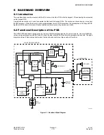


BASEBAND OVERVIEW
MCUK991001G8
Section 6
Issue 1
Technical Guide
– 21 –
Revision 0
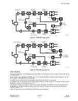
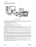
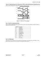
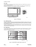
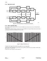
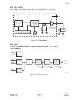
There are not enough general purpose I/O lines available on GEMINI, so eight additional signal lines are provided by the port
expander. To control the additional lines, the data bus lines D0 to D7 are used along with RnW and a dedicated nCS(0) line.
The ‘D’ inputs are clocked to the ‘Q’ outputs by an XOR function of RnW and nCS(0).
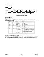
Figure 6.3: Port Expander Timing Diagram
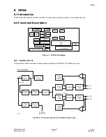
6.2.4 Time Processing Unit (TPU)
The TPU provides the GSM TDMA timing requirements for the system, external timing signals are provided by an area of
Microcode within the GEMINI chip.
6.2.5 CPU Memory
GD30/GD50 uses a Dual Operation (DL) Flash memory U502, comprising a 16 bit Flash ROM and 8 bit SRAM. DL Flash
memory is able to access one block of memory while writing another block of memory.
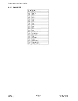
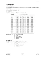
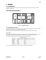
GEMINI Pin Description
65
VEGA BENA
71
VEGA BCAL
67
VEGA BULON
68
VEGA BDLON
69
RF PA_ON
70
RF PCNnGSM
118
RF signal RXON1
119
RF signal RXON2
58
VEGA_SEL
59
RF PLL_STRB
60
RF signal TXON
61
N.C.
62
RF IFAGCEN
RESET
nCS(0)
RnW
CLK
D
D0
D1
D2
D3
Q
D1
D3
NOTE:
CLK IS AN INTERNAL SIGNAL.
10158-1


