background image

2-4

Quick start

PC-510 user’s manual

WARNING!

Before the PC-510 is powered on, all eight standoffs, screws
and washers should be secured to the board.  The standoff
pieces will ensure full support of the PC-510 not only on all
four sides, but also in the middle of the board.  These hard-
ware pieces will reduce the circuit board flex when the
PC/104 expansion board and/or the SSD0 are inserted.  Flex-
ing of the PC-510 board should be avoided, since it can cause
problems with the copper circuit traces and the surface
mounted components.

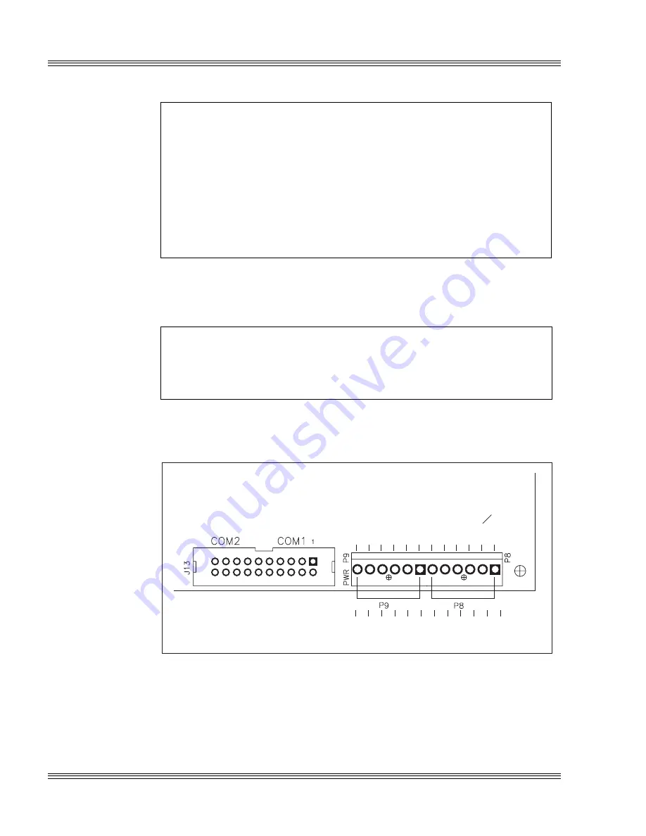
3. The power supply connector is located at P8, P9.  Make certain to

connect the ground wires (typically black) to all ground connectors at

P8, P9 on the PC-510.  Refer to Figure 2-3.

WARNING!

Accidently crossing the wires, i.e., pl5V wires into
the ground connector or the ground wires into the +5V
connector can damage the PC-510.

Figure 2-3

Power connector:  P8, P9

Red

Red

Red

White

Black

Black

Black

Black

Blue

Yellow

Red

Orange

Standard cable wire colors

P8, P9

Power header

+5V

+5V

+5V

–5V

Gnd

Gnd

Gnd

Gnd

–12V

+12V

+5V

NC

Note

By removing the keys on the PC-510, it is possible to key your power

connector header to your power supply connector.  To insert the power

connector without removing the keys, angle the connector at 90

° 

and

then place it on P8, P9.

Summary of Contents for PC-510

Page 1: ...tracting zip file located at the Octagon Systems web site on the product specific page Download this file to a separate directory on your hard drive then double click on it to extract the files All references in this manual to files and directories on the CD now refer to files in the Utilities zip file ...

Page 2: ...O C T A G O N S Y S T E M S Embedded PCs For Extreme Environments PC 510 User s Manual 5171 0505 ...

Page 3: ...hange without notice The information contained in this manual is believed to be correct However Octagon assumes no responsibility for any of the circuits described herein conveys no license under any patent or other right and makes no representations that the circuits are free from patent infringement Octagon makes no representation or warranty that such applications will be suitable for the use s...

Page 4: ... put in the context of the Micro PC Octagon has developed a reliable database of customer induced field failures The average MTBF of Micro PC cards exceeds 11 years yet there are failures Most failures have been identified as customer induced but there is a small percentage that cannot be identified As expected virtually all the failures occur when bringing up the first system On subsequent system...

Page 5: ... tances is 2 1 or greater fault conditions most likely have occurred A common cause is miswiring the power supply n Improper power causes catastrophic failure If a card has had reverse polarity or high voltage applied replacing a failed compo nent is not an adequate fix Other components probably have been partially damaged or a failure mechanism has been induced There fore a failure will probably ...

Page 6: ...on digital inputs Long leads act as an antenna to pick up noise They can also act as unterminated transmission lines When 5V is switch onto a line it creates a transient waveform Octagon has seen submicrosecond pulses of 8V or more The solution is to place a capacitor for example 0 1 µF across the switch contact This will also eliminate radio frequency and other high frequency pickup Avoiding phys...

Page 7: ...Notice to user PC 510 user s manual ...

Page 8: ...4 Diagnostic software verifies system integrity automatically 1 5 SETUP information stored in EEPROM for high reliability 1 5 Phoenix BIOS 1 5 Instant DOS operating system 1 5 Programmable video BIOS 1 5 On board flash file system 1 6 Octagon BIOS extensions 1 6 Interrupt routing In system and programmable 1 6 Floppy and hard disk ports 1 6 Boot sequence 1 6 Multifunctional printer port 1 6 Watchd...

Page 9: ...t options 5 1 Description of serial ports 5 2 Conflicting COM port addresses 5 2 COM1 5 2 COM2 5 3 COM3 through COM6 interrupt status port 5 3 COM3 5 5 COM4 5 5 COM5 5 5 COM6 5 6 Null modem cable 5 6 Building your own cable 5 7 Function and use of serial ports 5 9 COM1 as serial console device 5 9 COM1 through COM6 as RS 232 I O 5 9 COM5 as GPS I O 5 9 COM6 RS 485 transmitter control 5 10 RS 485 n...

Page 10: ...rements 9 1 Installing a floppy disk drive 9 1 Hard disk controller 9 2 Installing a hard drive 9 2 Booting with ROM DOS 9 2 Chapter 10 IRQ routing and opto IRQs 10 1 Interrupt routing 10 1 Opto IRQs 10 3 Interrupt routing matrix defaults 10 3 Programming 10 3 Master disable 10 4 Chapter 11 EZ I O 11 1 Description 11 1 EZ I O options 11 2 Pulling the I O lines high or low 11 2 Organization of port...

Page 11: ...4 2 GPS interface port options 14 3 Routing the GPS data 14 3 Chapter 15 PC 104 expansion 15 1 Description 15 1 Overview Section 3 System management Chapter 16 Watchdog timer and hardware reset 16 1 Description 16 1 Enhanced INT 17h function definitions 16 1 Enable watchdog 16 1 Strobe watchdog 16 2 Disable watchdog 16 2 Hardware reset 16 3 Chapter 17 Serial EEPROM and CMOS RAM 17 1 Description 17...

Page 12: ...es of the PC 510 SSD 19 5 Programming copies of the PC 510 SSD 19 5 Programming a new BIOS into SSD1 19 6 Programming the video BIOS into an SSD 19 6 Chapter 20 User defined jumper 20 1 User defined jumper 20 1 Read jumpers 20 1 Chapter 21 CPU power management 21 1 Description 21 1 Power management overview 21 1 Hardware controlled modes 21 2 Device power management 21 2 System power management 21...

Page 13: ... I17HNDLR EXE B 5 LCDBIAS EXE B 6 LPT1CON COM B 7 PFORMAT EXE B 8 PGMBIOS EXE B 8 PGMIMG EXE B 9 PGMIMGH EXE B 10 PGMVIDEO EXE B 11 PHDISK EXE B 12 PICOFA SYS B 13 PMISETUP EXE B 14 REMDISK EXE B 15 REMQUIT COM B 17 REMSERV EXE B 17 RESET COM B 19 SCONSOLE EXE B 19 SETIRQ EXE B 20 SETSSD EXE B 20 SETUP COM B 22 TESTRFA EXE B 23 TRANSFER EXE B 24 VDISK SYS B 26 Appendix C Third party support C 1 Us...

Page 14: ...al console 7 2 Figure 7 2 VTC 20F cable and null modem adapter 7 2 Figure 7 3 Changing ROM Enable flowchart 7 4 Figure 10 1 Interrupt routing matrix 10 2 Figure 11 1 Typical EZ I O configurations 11 1 Figure 11 2 Organization of ports 11 3 Figure 11 3 MPB 16PC opto rack hookup 11 12 Figure 11 4 PC 510 interfacing with an STB 26 terminal board 11 14 Figure 13 1 The PC 510 a VGA monitor and an AT PS...

Page 15: ...5 6 Table 5 11 Available addresses for COM6 at port 0A9h IRQ 15 default routable 5 6 Table 5 12 Custom RS 232 null modem cable for the PC 510 First COM port 5 7 Table 5 13 Custom RS 232 null modem cable for the PC 510 Second COM port 5 8 Table 5 14 RS 485 transmitter control COM6 at location 32Ch 5 10 Table 5 15 RS 485 termination select jumper W1 5 10 Table 7 1 Video BIOS disabling and enabling o...

Page 16: ...d shift clock signal voltage level select W9 A 7 Table A 16 Power connector P8 P9 A 8 Table A 17 Speaker connector J1 A 8 Table A 18 Keyboard connector J2 A 8 Table A 19 Mouse connector J3 A 9 Table A 20 AT and industrial serial for COM3 and COM4 J4 A 9 Table A 21 AT and industrial serial for COM5 and COM6 J5 A 10 Table A 22 LPT1 as printer connector J6 A 11 Table A 23 AT and industrial serial for...

Page 17: ...xii Contents PC 510 user s manual ...

Page 18: ...ch as analog input output digital input output motion control and display EZ I O This digital I O chip supplies 24 I O lines which can be individually programmed as 5V input or 5V output h The suffix h denotes a hexadecimal number A decimal number has no prefix or suffix For ex ample 1000h and 4096 are equivalent KB Kilobyte 1 024 8 bit bytes MB Megabyte 1 048 576 8 bit bytes Memory device The typ...

Page 19: ... memory EEPROM or static RAM Static RAM Static Random Access Memory device Static RAMs provide volatile memory with unlimited read and write cycles They may be used with a backup battery TTL compatible Transistor transistor logic compatible 0 5V logic levels Virtual drive A disk created in DOS or extended memory which emulates an actual disk The virtual drive provides temporary storage for files W...

Page 20: ...er a single keyword for example reset For most commands however you will enter several keywords followed by one or more parameters for which you must supply values Commands must be entered in a specific format To indicate the format this manual uses a series of conventions that are explained below The conventions cover the rules for issuing all commands including the most complex ones Most command...

Page 21: ... to your particular system or program e g Enter filename means enter the name of your file n Paired angle brackets are used to indicate a specific key on your keyboard e g ESC means the escape key CTRL means the control key F1 means the F1 function key n All addresses are given in hexadecimal for example 328h ...

Page 22: ...M and battery backup Chapter 9 External drives Chapter 10 IRQ routing and opto IRQs Chapter 11 EZ I O Chapter 12 LED signaling and beep codes Chapter 13 CRTs and flat panels Chapter 14 GPS interface Chapter 15 PC 104 expansion n Section 3 System management Chapter 16 Watchdog timer and hardware reset Chapter 17 Serial EEPROM and CMOS RAM Chapter 18 Transferring files remote disks Chapter 19 Managi...

Page 23: ...About this manual PC 510 user s manual ...

Page 24: ...nstallation Section 1 provides installation and programming instructions startup options and system configuration program examples The following chapters are included Chapter 1 Overview Chapter 2 Quick start Chapter 3 SETUP programs Chapter 4 Save and run programs ...

Page 25: ...Overview of Section 1 PC 510 user s manual ...

Page 26: ... version of the PC 510 is listed below with the standard and optional features The standard version can be used for system development and an optional version of the PC 510 is usually application specific PC 510 major hardware features CPU The high performance 586 CPU comes in two versions One version is a 120MHz586 and the other is a 133MHz586 Both versions operate at 3 3V for low power consumpti...

Page 27: ...pport from SRAM optional For information on changing the device type refer to the W5 SSD0 table in the Quick start chapter You can also install compatible PROMs into SSD0 through the supplied utility programs found on the PC 510 utility disk You can format the flash or SRAM while in the socket EPROM usage however requires off card programming from either a master flash or a master SRAM SSD1 SSD1 i...

Page 28: ...COM1 through COM6 standard n Omission of COM3 through COM6 optional Local bus SVGA flat panel interface and GUI accelerator The video system on the PC 510 uses the advanced 65550 video chip from Chips Technologies It supports CRT LCD and EL displays with resolutions to 1280 x 1024 bpp Displays from CGA through SVGA are supported The 65550 is also a graphics accelerator with real time PC video bein...

Page 29: ...rd The mouse port is optional and follows the PS 2 standard Neither the keyboard nor the mouse are required for operation n Mouse port included standard n Mouse port not included optional PC 104 16 bit interface This interface is a standard feature on the PC 510 and accepts an 8 or a 16 bit PC 104 expansion board PC 104 expansion boards are avail able from several manufacturers As many as three PC...

Page 30: ...n EEPROM for high reliability Loss of SETUP data is serious in industrial applications Most PCs store SETUP information in battery backed CMOS RAM If the battery fails or is replaced during routine maintenance this information is lost Without a keyboard and monitor in embedded applications time con suming re initialization is required The PC 510 stores the SETUP information in EEPROM with 1 536 by...

Page 31: ...sion card Floppy and hard disk ports The floppy disk port supports two drives with either 720 KB or 1 44 MB capacities The floppy port is terminated with a 34 pin IDC connector The EIDE hard drive port is terminated with a 44 pin 2 mm connector 5V is supplied to a 2mm hard drive through the EIDE connector and 5V is also optionally supplied to the floppy drive through the IDC connector Boot sequenc...

Page 32: ...For embedded applications the parallel printer port or the EZ I O port can interface with a 16 key matrix keypad and a 2 or 4 line LCD dis play The PC 510 is supplied with software that provides keypad scan ning and display operation Supplied display and keypad drivers in C support these devices Hardware reset A hardware reset can be done by any of the following methods n Issuing the RESET softwar...

Page 33: ...the Power supply requirements section in the Quick start chapter for more information on power supply selection and criteria Rugged environmental operation n Operating temperature 40 to 70 C operating with adequate airflow n Nonoperating temperature 55 to 90 C nonoperating n Relative humidity 5 to 95 noncondensing n Altitude 100 to 10 000 m n Shock 10g 3 axis n Vibration 3g 3 axis Note Forced air ...

Page 34: ...nt diagram Figure 2 1 for the location of various connectors before installing your PC 510 system WARNING The PC 510 Mobile Industrial Computer contains static sensi tive CMOS components Do the following to avoid damaging your card and its components n Ground yourself before handling the PC 510 card n Disconnect power before removing or inserting a PC 104 expansion card n When programming a memory...

Page 35: ...2 2 Quick start PC 510 user s manual Figure 2 1 PC 510 component diagram ...

Page 36: ...2 3 PC 510 user s manual Quick start Figure 2 2 PC 510 center to center hole dimensions 331 2 858 ...

Page 37: ...e power supply connector is located at P8 P9 Make certain to connect the ground wires typically black to all ground connectors at P8 P9 on the PC 510 Refer to Figure 2 3 WARNING Accidently crossing the wires i e plugging 5V wires into the ground connector or the ground wires into the 5V connector can damage the PC 510 Figure 2 3 Power connector P8 P9 Red Red Red White Black Black Black Black Blue ...

Page 38: ... 5V 6 Gnd 6 5V Note See the Accessories appendix for connector information on the power connector 4 Connect the PS 2 style keyboard directly to the keyboard port at J2 and a VGA monitor to J20 using a VGA 12 cable Refer to Figure 2 4 Figure 2 4 PC 510 keyboard and monitor VGA 12 cable PC 510 Keyboard connector J2 Mouse connector J20 Keyboard cable VGA Monitor ...

Page 39: ...er J18 Battery J7 COM1 COM2 J19 PC Video J9 Floppy disk drive J20 SVGA CRT analog J10 IDE hard drive P8 P9 Power J11 PC 104 J12 N A Note See the Accessories appendix for connector information on the above connectors Table 2 3 RS 485 termination select jumper W1 Pins Description 1 2 No function used for shunt storage 3 4 No function used for shunt storage 5 6 No function used for shunt storage 7 8 ...

Page 40: ...liary option jumper W3 Pins Label Description 1 2 V1 C8000 CFFFF BIOS region toggle video BIOS region 2 3 4 X D8000 DFFFF BIOS region toggle PICO FA 5 6 U2 User option jumper 2 7 8 VE VGA controller on enabled off disabled 9 10 I IRQ matrix on disabled off enabled factory default pins jumpered Toggles in BIOS extension areas work in combination with toggles in the SETUP BIOS extension areas See th...

Page 41: ...ignal voltage level select W9 Pins Description 1 2 3 3V 3 4 5V default pins jumpered PC 510 power supply requirements The PC 510 is designed to operate from a single 5VDC supply An AT compatible power supply connector header P8 P9 is on board and ensures the required number of power and ground paths from the power supply Make sure that you utilize all three 5 VDC conductors and all four ground con...

Page 42: ...he proper selection of a quality power supply ensures reliability and proper functioning of the PC 510 WARNING Make sure the power supply is OFF when connecting the power cable to the PC 510 board Damage to the PC 510 may occur if the power is ON when connecting the power cable Running a demo program Logon message 1 Power on the PC 510 2 A logon message similar to the one below appears on your PC ...

Page 43: ... all jumpers are set to factory defaults Refer to the Technical data appendix for all default jumper settings n If the system still does not respond remove W2 9 10 to run BIOS default SETUP and try again Also refer to the Troubleshooting chapter 3 Use the directory command to make sure your equipment and software are working properly Enter PC510 C DIR A directory listing of files stored in the SSD...

Page 44: ...he SETUP programs chapter 2 To connect a floppy and or hard drive see the External drives chapter 3 Refer to the Transferring files remote disks chapter to transfer files from a host PC and to use a remote disk via a serial connection 4 To use a serial console refer to the Console devices chapter ...

Page 45: ...2 12 Quick start PC 510 user s manual ...

Page 46: ...can be entered in one of two ways n Run SETUP COM n Press the backspace key followed by the S key during BIOS POST sequence this occurs between the memory test and boot Also by removing the USESETUP jumper from W2 9 10 you may force the setup to temporarily revert to the BIOS defaults Table 3 1 and also allow the user to reconfigure the setup options The SETUP program defines the PC 510 system par...

Page 47: ...evice C Only Serial port COM1 Specifies COM1 enable disable Enabled Serial port COM1 address COM1 address 3F8h Serial port COM2 Specifies COM2 enable disable Enabled Serial port COM2 address COM2 address 2F8h Parallel LPT port Specifies LPT port enable disable Enabled Parallel port mode Specifies mode to use with parallel port Bidirectional printer port Parallel port address Specifies address to u...

Page 48: ... via hotkey Specifies backspace S hotkey enable disable Enabled Power management Specifies power management enable disable Enabled Doze clock Specifies doze mode in power management is to slow or stop the clock Slow Time update after suspend Specifies to allow update of time after suspend mode Enabled DIMM module type Specifies the type of DIMM module EDO ROM Enable Toggles video BIOS region first...

Page 49: ...etup parameters and available options Select the option by pressing the space bar until the correct information appears then press ENTER Press ESC twice if you want to exit SETUP without saving your responses Note Options having an are default settings n Serial Console on COM1 ENABLED DISABLED WARNING Disabling the serial console when there is no video monitor present will stop further serial cons...

Page 50: ...recommend the use of bidirectional mode EPP and ECP modes are provided for equip ment that has the capability to operate in these modes for enhanced performance n Number of floppy drives 0 1 2 C Only A Then C n Serial Port COM1 Enabled Disabled n Serial Port COM1 address 3F8h 2F8h 338h 3E8h 2E8h 220h 238h 2E0h 228h n Serial Port COM2 Enabled Disabled n Serial Port COM2 address 2F8h 338h 3E8h 2E8h ...

Page 51: ...bled Disabled n Parallel Port Mode Bidirectional mode EPP mode ECP mode Standard Unidirectional mode n Parallel Port Address 378h 278h 3BCh n IRQ for LPT port IRQ7 IRQ5 n Onboard floppy controller Enabled enables onboard floppy connector J9 Disabled n Drives A and B No requires a swap in the cable Yes does not require a swap in the cable n Floppy drive 1 size Not Installed 5 25 360 KB 5 25 1 2 MB ...

Page 52: ... xx Sectors xx n Internal CPU cache Enabled Disabled n Limit CPU to half speed NO YES n Setup entry via hotkey Enabled Disabled n Power management Enabled Disabled n Doze clock Slow Stop n Time update after suspend Enabled Disabled n DIMM module type EDO Standard n Shadow C0000h C7FFFh Disabled Enabled n Shadow C8000h CFFFFh Disabled Enabled n Shadow D0000h D7FFFh Disabled Enabled ...

Page 53: ...CEPT ESC to EXIT Serial Console on COM1 ENABLED COM1 Console Baud Rate 9600 Power on memory test DISABLED Boot Sequence C ONLY Serial Port COM1 ENABLED Serial Port COM1 Address 3F8h default Serial Port COM2 ENABLED Serial Port COM2 Address 2F8h default Parallel LPT Port ENABLED Parallel Port Mode Bidirectional Printer Port Parallel Port Address 378h Number of floppy drives 1 Onboard Floppy Control...

Page 54: ... take effect PC510 C Note Executing SETUP D will change all setup parameters to default values SETSSD For more information on SETSSD refer to the Defining SSDs using SETSSD section in the Managing SSDs chapter PMISETUP PMISETUP allows the user to customize the power management fea tures of the PC 510 Refer to the CPU power management chapter See also the Software utilities appendix for details SET...

Page 55: ...3 10 SETUP programs PC 510 user s manual ...

Page 56: ... Microsoft programs make undocumented DOS calls With ROM DOS an error returns when an undocumented DOS call is made causing your program to operate erratically We recom mend booting from SSD1 using your own DOS when using programs with undocumented DOS calls Refer to the section Adding operating system startup files in the Managing SSDs chapter for more information on saving and autoexecuting prog...

Page 57: ...e drivers to your drive as well 3 To autoexecute your application add your application name to the AUTOEXEC BAT file To replace our example program DEMO EXE with your application substitute DEMO in the AUTOEXEC BAT file with your applications filename Autoexecuting your application This section describes how to autoexecute your application 1 To autoexecute your application in SSD1 use the SETSSD c...

Page 58: ...one of the following options Option 1 1 Press F5 or F8 on your local keyboard For more information see your ROM DOS manual Option 2 1 Change AUTOEXEC BAT and or CONFIG SYS to not call out your program Option 3 1 Install a floppy 2 Change SETUP option Boot Sequence to A THEN C 3 Change SETUP to enable the floppy 4 Boot from floppy 5 Change AUTOEXEC BAT on C ...

Page 59: ...4 4 Save and run programs PC 510 user s manual ...

Page 60: ...eatures The following chapters are included Chapter 5 Serial ports Chapter 6 LPT1 parallel port Chapter 7 Console devices Chapter 8 SSDs DRAM and battery backup Chapter 9 External drives Chapter 10 IRQ routing and opto IRQs Chapter 11 EZ I O Chapter 12 LED signaling and beep codes Chapter 13 CRTs and flat panels Chapter 14 GPS interface Chapter 15 PC 104 expansion ...

Page 61: ...Overview of Section 2 PC 510 user s manual ...

Page 62: ...rates up to 115 2K All ports have the following specifications 16C550 compatible 16 byte FIFO buffers IEC 1000 level 3 ESD protection Contact discharge 6 kV Air gap discharge 8 kV Backdrive protection Up to 115 2k baud operation 5 6 7 or 8 bit word lengths 1 1 5 or 2 stop bits Serial port options The standard version PC 510 has COM1 and COM2 installed as an 8 wire interface Under OEM contract you ...

Page 63: ...iguration The I O address for COM1 is 3F8h default but can be changed in SETUP to any of the addresses in the table below Refer to the SETUP programs chapter for more informa tion on running SETUP IRQ4 is dedicated to COM1 and if COM1 is not used under interrupt control IRQ4 may be used by other resources For example when COM1 is the console COM1 uses IRQ4 COM1 can be used for console I O or RS 23...

Page 64: ...esources such as the PC 104 expansion board the GPS module IRQ routing etc Refer to the IRQ routing and opto IRQs chapter for details COM1 and COM2 share the J7 20 pin header Table 5 4 COM2 available addresses IRQ3 dedicated COM2 available addresses Note See the Accessories appendix for connector information on COM1 and COM2 COM3 through COM6 interrupt status port COM3 through COM6 share the same ...

Page 65: ... read the interrupt status port Bit 0 through bit 3 show which serial port caused the interrupt For example when there is a 1 in bit 3 this means COM3 caused the interrupt a 1 in bit 2 shows that the interrupt came from COM4 a 1 in bit 1 means that COM5 caused the interrupt and by default when a 1 is in bit 0 then COM6 caused the interrupt See the table above to read the interrupt status port Note...

Page 66: ...der For more information see the COM3 through COM6 interrupt status port section in this chapter Table 5 9 COM4 available address and IRQ routing Address IRQ Z q Note See the Accessories appendix for connector information on COM3 and COM4 COM5 COM5 functions either as an RS 232 serial port or as a global position ing system GPS module port Both configurations are standard features and may be omitt...

Page 67: ...8h through the interrupt routing matrix The interrupt for COM6 is logically OR d with COM3 through COM5 COM5 and COM6 share J5 20 pin header For more information see COM3 through COM6 interrupt status port section in this chapter Table 5 11 Available addresses for COM6 at port 0A9h IRQ 15 default routable I O range select A bit 5 I O range select B bit 4 COM6 addresses RS 485 transmitter control b...

Page 68: ...RxD and TxD signal are crossed Cable pins 4 and 6 in the first COM port connector of the PC 510 are tied together and cable pins 14 and 16 in the second COM port connector of the PC 510 are tied to gether Pins 7 and 8 are tied together on each DB 9 cable connector Pins 4 and 5 are tied together on each DB 25 cable connector Refer to the following table and diagram for a complete listing of all cab...

Page 69: ...nal DB 9 pin DB 25 pin PC port signal Z Z _ Figure 5 2 Custom null modem cable for the PC 510 First COM port Second COM port DB 9 DB 9 DCD DSR RxD RTS TxD CTS DTR RI GND 5V Safe 1 2 3 4 5 6 7 8 9 10 DCD DSR RxD RTS TxD CTS DTR RI GND 5V Safe 11 12 13 14 15 16 17 18 19 20 1 2 3 4 5 6 7 8 9 1 2 3 4 5 6 7 8 9 DCD RxD TxD DTR GND DSR RTS CTS RI DCD RxD TxD DTR GND DSR RTS CTS RI ...

Page 70: ...COM1 through COM6 as RS 232 I O COM1 through COM6 can also be used as RS 232 serial ports Depend ing upon the design of each port COM1 through COM4 can support 4 or 8 wire configurations and COM5 and COM6 are 4 wire only configurations Use a VTC 20F cable to interface from the PC 510 and the serial device Figure 5 3 PC 510 serial devices PC 510 COM6 COM5 COM4 COM3 COM2 COM1 Serial device Serial de...

Page 71: ...ntrol toggle bit 1 of base address 4 32Ch Refer to the following table on RS 485 terminations Table 5 14 RS 485 transmitter control COM6 at location 32Ch Program statement Description q q q q q q Note The above address at COM6 for the RS 485 transmitter control may change Refer to Table 5 11 for a complete listing of COM6 addresses The RS 485 port is configured for termination for either marking o...

Page 72: ...5 network there can only be one host The host is responsible for initiating communi cation maintaining network registration and providing housekeep ing tasks with other nodes Remotes however cannot initiate a communication They can only respond to messages that are ad dressed to them from the host The following diagram demonstrates how a typical two wire trans mission is implemented in the RS 485 ...

Page 73: ...5 12 Serial ports PC 510 user s manual ...

Page 74: ...matrix keypad or an opto rack with opto isolated digital I O modules Note Make sure that the interrupt used for COM3 through COM6 does not conflict with the IRQ selected for the LPT in SETUP Printer The following table illustrates the pinout for the LPT1 parallel port used as a printer port Note See the Accessories appendix for connector information on the LPT1 printer port connector Installing a ...

Page 75: ...her the 14 pin or 16 pin header on the 2010 The size of the display will determine which header to use 3 Refer to the file DISPLAY DOC for more information on initializing and using the display Keypad LPT1 also supports 4 x 4 matrix keypads To interface the keypad to the PC 510 use the Octagon 2010 interface board A CMA 26 cable is required to connect the interface board to the PC 510 The program ...

Page 76: ...control high voltage high current G4 opto isolated modules Of the sixteen positions available eight can be either input or output four are dedicated as inputs and the other four are dedicated as outputs Refer to the MPB 16PC opto module rack product sheet for more information Figure 6 3 LPT1 and an opto rack LPT1 parallel port CMA 26 ribbon cable MPB 16PC opto rack 32 J2 J2 1 2 7 6 5 4 3 8 9 14 13...

Page 77: ...6 4 LPT1 parallel port PC 510 user s manual ...

Page 78: ... serial cable null modem adapter plugged into a host PC running SmartLINK provides both input and output The local keyboard also allows input n No console device means no video output either from the SVGA moni tor or the serial console The local keyboard allows input Local bus SVGA For correct usage of the CRT and flat panel see the CRTs and flat panels chapter Serial console If the serial console...

Page 79: ... your PC has a 25 pin serial connector attach a 9 to 25 pin adapter to the 9 pin null modem adapter and then insert the matching end of the 9 to 25 pin adapter into the serial port 6 Start PC SmartLINK 7 Remove W2 1 2 and W3 1 2 to disable the video BIOS Note For more information on enabling and disabling the video BIOS refer to the following section in this chapter 8 Power on the PC 510 Figure 7 ...

Page 80: ...ne which console device to use If a console device exists the BIOS will use the console device the CRT or the flat panel When the console device does not exist the BIOS will otherwise use a serial console if it has not been disabled in SETUP To enable disable the video BIOS area either change W2 1 2 W3 1 2 or run SETUP and change C0000h C7FFFh or C8000h CFFFFh ROM enable options The jumpers work a...

Page 81: ...Off Enabled Change SETUP to enabled or install W2 1 2 V0 W3 1 2 V1 Enabled On Disabled Change SETUP to disabled or remove W2 1 2 V0 W3 1 2 V1 Enabled Off Disabled Change SETUP to disabled or install W2 1 2 V0 W3 1 2 V1 Note Octagon strongly recommends that you configure both the ROM Enable SETUP option and the jumpers W2 1 2 and W3 1 2 at the same time Figure 7 3 Changing ROM Enable flowchart YES ...

Page 82: ...ESETUP W2 9 10 2 Install W2 1 2 W3 1 2 3 Reboot the system If Step A does not work then follow Step B Step B 1 Make sure the BIOS jumper W2 5 6 is on To use the BIOS in SSD1 install W2 5 6 To use the BIOS in SSD0 remove W2 5 6 2 Reboot the system If Step B does not work then follow Step C Step C 1 Remove W2 1 2 W3 1 2 2 Attach a serial cable to COM1 3 Run PC SmartLINK at 9600 baud 4 Boot the syste...

Page 83: ...7 6 Console devices PC 510 user s manual ...

Page 84: ...EPROM device may be installed on the PC 510 Jumper blocks W2 7 8 and W5 must be set appropriately See Table 8 1 for settings Selecting SSD0 device type Table 8 1 SSD0 device selection jumpers W5 W2 7 8 Pins Description W5 1 3 2 4 5 7 8 10 W2 7 8 SRAM with battery backup W5 1 2 3 4 5 6 9 10 W2 7 8 Flash W5 1 2 3 4 5 6 9 10 EPROM default pins jumpered W2 7 8 is not jumpered SSD0 replaced with an SRA...

Page 85: ...ives on SSD0 to be the full size 512 KB WARNING Alignment of an SRAM flash or EPROM device into SSD0 is critical Be certain to properly align pin 1 of either the SRAM flash or EPROM device with pin 1 of SSD0 on the PC 510 SSD0 replaced with a flash device Before replacing SSD0 with a flash device do the following steps 1 Power off the PC 510 and then make sure W2 5 6 is jumpered in order to boot f...

Page 86: ... Your application programs can be saved to flash using the PICO FA driver which makes the flash device a read write disk on your PC 510 Saving your programs onto the read write disk allows you to do this up to 100 000 times allowing updates to your application programs These devices are erased automatically during the programming process SSD1 can be accessed directly as a read write DOS drive with...

Page 87: ...G02TB 8 MB EDO DIMM Octagon 4584 memory module IBM IBM11S2325LPB 70 Kingston KTM2X32V 70DEG PNY Engineering 322007EDM1G04TB 16 MB EDO DIMM Octagon 4582 memory module IBM IBM11S4325LPB 70 PNY Engineering 324007EDS4G08TL 32 MB EDO DIMM Octagon Call Octagon memory module Battery backup for SSD0 SRAM and real time calendar clock Located at J18 the AT battery backs up the CMOS real time clock and SSD0 ...

Page 88: ...cable which has two connectors Power requirements The PC 510 requires 5V for operation You must also supply power to the floppy drive s through an external source Refer to your floppy drive manual for specific instructions Installing a floppy disk drive 1 Disconnect power to the PC 510 2 Insert one end of your cable into the rear of the floppy drive Make sure pin 1 on the cable is connected to pin...

Page 89: ...he PC 510 Make sure pin 1 on the cable is connected to pin 1 on the PC 510 4 Execute the BIOS SETUP program to configure your system for a hard drive You can execute this program either by pressing BACK SPACE S during system bootup or by executing the file SETUP EXE This file is found on the PC 510 BIOS drive and the PC 510 utility disk The system steps you through the configuration Also refer to ...

Page 90: ...program to update the routing matrix with the desired IRQ routes In addition to IRQ routing the I O range select A and select B bits can be set so that the base addresses in COM5 and COM6 EZ I O 1 and EZ I O 2 and COM3 through COM6 IRQ status registers can be moved to different locations These can also be read at I O address 0A9h bits 4 and 5 See also the SETIRQ DOC file in the IRQ directory on th...

Page 91: ...RxD RS 232 COM6 Programming Control D e s t i n a t i o n Opto Isolators OPTOB OPTOA Reset Power Supervisor PMI Sus Rsm Power Management TMARK GPS Mouse IRQ COM3 4 5 6 IRQ BUS IRQ3 BUS IRQ4 BUS IRQ5 BUS IRQ7 BUS IRQ11 S o u r c e RxD RS 485 COM6 COM5 Receive Data RxD COM5 COM6 Receive Data RxD COM6 Primary IDE Interrupt Controller BUS IRQ9 BUS IRQ6 IRQ1 IRQ2 IRQ9 IRQ13 IRQ6 IRQ8 IRQ3 IRQ4 IRQ5 IRQ...

Page 92: ...put voltage remains stable until the interrupt is acknowledged At that time the interrupt source can be rearmed by returning the input to 0 volts Note See the Accessories appendix for mating information on the OPTOA and OPTOB connectors The interrupt routing matrix provides flexibility to the interrupt struc ture which allows connection between the lower ordered ISA interrupts and the unused highe...

Page 93: ...OC for more information The IORG SEL A I O register select A and IORG SEL B I O register select B select the base address for serial ports 5 and 6 as well as for the EZ I O and the interrupt status register Table 10 1 Interrupt status port ISP map setting at I O location 0A9h I O range select A bit 5 I O range select B bit 4 COM5 COM6 EZ I O 1 EZ I O 2 Interrupt status register 0 1 120 127h 128 12...

Page 94: ...orts have the following specifications n Each EZ I O chip has 24 I O lines grouped into 3 ports of 8 bits n 48 I O lines available n Each bit is programmable as either 5V input or 5V output n Read back state of each pin n Easy to program n Each line can sink and source 15 mA Figure 11 1 Typical EZ I O configurations MPB Opto Rack J1 J2 P8 1 2 7 6 5 4 3 8 9 14 13 12 1 1 10 15 16 LOGIC 0 1 2 3 4 5 6...

Page 95: ... lines Under OEM contract the EZ I O ports can be eliminated or only one port can be installed for 24 I O lines Table 11 2 EZ I O port options Standard feature Option 1 Option 2 EZI O 1 Installed Installed Not installed EZI O 2 Installed Not installed Not installed Total I O lines 48 24 0 Note See the Accessories appendix for connector information for the EZ I O 1 and EZ I O 2 connectors Pulling t...

Page 96: ...jumpered Organization of ports Each EZ I O digital port has a total of 24 I O lines connected to a 26 pin header The lines are configured into three groups ports A B and C each group consisting of 8 bits Any of the lines at ports A B or C can be configured individually as inputs or outputs Figure 11 2 Organization of ports Base Base 1 Base 2 Base 3 A B C EZ I O digital I O chip 8 8 Control Registe...

Page 97: ...d EZ I O 2 port addresses at I O location 0A9h I O range select A bit 5 I O range select B bit 4 EZ I O 2 base address EZ I O 1 base address 0 1 130 133h 134 138 0 0 150 153h 154 158 1 0 350 353h 354 358 1 1 330 333h 334 338 default settings Configuring and programming the EZ I O ports J15 and J16 the digital I O connectors each have an Octagon EZ I O digital chip associated with them The EZ I O c...

Page 98: ... 333h 2 control register direction mode 2 Set the direction of each bit A 0 written to the corresponding line indicates an input and a 1 bit indicates an output Each bit corre sponds to the equivalent I O line Table 11 6 EZ I O port byte bit 7 bit 6 bit 5 bit 4 bit 3 bit 2 bit 1 bit 0 EZ I O port I O line x 7 x 6 x 5 x 4 x 3 x 2 x 1 x 0 For example writing 00011100 to port C base address 2 will co...

Page 99: ...mands OUT 333h 2 Direction Mode OUT 330h FFh PortA OUT 331h FFh PortB OUT 332h FFh PortC OUT 333h 3 Operation Mode Note With CAMBASIC Octagon s multitasking industrial language you can also accomplish the same configuration and outputs with one statement Enter CONFIG EZ I O 330 0 FF 0 FF 0 FF Ports A B and C will now output all 1 s after issuing the following commands OUT 330h FFh portA OUT 331h F...

Page 100: ...ort A xxxxxxxxB direction 1 output 0 input BX Port B configuration xxxxxxxx xxxxxxxxB xxxxxxxx Initial data for port B xxxxxxxxB direction 1 output 0 input CX Port C configuration xxxxxxxx xxxxxxxxB xxxxxxxx Initial data for port C xxxxxxxxB direction 1 output 0 input DX ffffh Return registers Carry flag cleared if successful Carry flag set if error AL Error code Comments This function is used to ...

Page 101: ...for port C 1 bit to be changed xxxxxxxxB Data for port C DX ffffh Return registers Carry flag cleared if successful Carry flag set if error AL Error code Comments This function is used to initialize the first EZ I O i e the EZ I O that has the higher I O address when two EZ I O chips are present on a board Programming example Inline assembly code for Borland C 3 1 asm mov ax 0ef01h mov di 00ffh po...

Page 102: ...unsigned char aData bData cData asm mov ax 0ef02h mov dx 0ffffh int 17h mov aData al mov bData ah mov cData bl Initialize EZ I O 2 Function efh Subfunction 03h Purpose To set the directions and to program the initial values of an EZ I O port Calling registers AH efh AL 00h DI Port A configuration xxxxxxxx xxxxxxxxB xxxxxxxx Initial data for port A xxxxxxxxB direction 1 output 0 input BX Port B con...

Page 103: ...fh Subfunction 04h Purpose To write a value to an EZ I O port Calling registers AH efh AL 04h DI Port A mask and data xxxxxxxx xxxxxxxxB xxxxxxxx Mask for port A 1 bit to be changed xxxxxxxxB Data for port A BX Port B mask and data xxxxxxxx xxxxxxxxB xxxxxxxx Mask for port B 1 bit to be changed xxxxxxxxB Data for port B CX Port C mask and data xxxxxxxx xxxxxxxxB xxxxxxxx Mask for port C 1 bit to b...

Page 104: ... flag set if error AL Error code Comments This function is used to read from the second EZ I O i e the EZ I O that has the lower I O address when two EZ I O chips are present on a board Programming Example Inline assembly code for Borland C 3 1 unsigned char aData bData cData asm mov ax 0ef05h mov dx 0ffffh int 17h mov aData al mov bData ah mov cData bl Opto module rack interface You can interface...

Page 105: ...pto rack diagrams below For either configuration run a separate power line to 5V and ground on the opto rack Figure 11 3 MPB 16PC opto rack hookup CMA 26 ribbon cable MPB 16PC opto rack EZ I O 1 EZ I O 2 J2 J2 1 2 7 6 5 4 3 8 9 14 13 12 11 10 15 16 0 1 2 3 4 5 6 8 P8 LOGIC J1 17 18 23 22 21 20 19 24 25 30 29 28 27 26 31 32 9 10 11 12 13 14 15 16 PC 510 Use the following table to determine the corr...

Page 106: ...2 14 bit 6 20 15 bit 7 18 Opto module position Port B 16 bit 0 10 17 bit 1 8 18 bit 2 4 19 MPB 24 bit 3 6 20 bit 4 1 21 bit 5 3 22 bit 6 5 23 bit 7 7 Interfacing to switches and other devices The STB 26 terminal board provides a convenient way of interfacing switches or other digital I O devices to the EZ I O digital port I O lines at the EZ I O connector can be connected to an STB 26 with a CMA 2...

Page 107: ...11 14 EZ I O PC 510 user s manual Figure 11 4 PC 510 interfacing with an STB 26 terminal board EZ I O 2 EZ I O 1 STB 26 terminal board J2 J1 PC 510 ...

Page 108: ... the boot sequence visual beep codes are dis played to the LEDs The visual beep codes are defined in the following table Also if a speaker is installed at J1 the beep codes are audible The bicolor LED also indicates memory suspend status Upon entering memory suspension the green LED turns off and the amber LED turns on On a resume condition the amber LED turns off and the green LED turns on When t...

Page 109: ...st 64K RAM parity test in progress or failure 10h 2 1 1 1st 64K RAM chip or data line failure bit 0 11h 2 1 2 1st 64K RAM chip or data line failure bit 1 12h 2 1 3 1st 64K RAM chip or data line failure bit 2 13h 2 1 4 1st 64K RAM chip or data line failure bit 3 14h 2 2 1 1st 64K RAM chip or data line failure bit 4 15h 2 2 2 1st 64K RAM chip or data line failure bit 5 16h 2 2 3 1st 64K RAM chip or ...

Page 110: ...lieved running w video ROM 31h N A Monochromatic screen believed operable 32h N A 40 column color screen believed operable 33h N A 80 column color screen believed operable 34h 4 2 1 Timer tick interrupt test in progress or failure 35h 4 2 2 Shutdown test in progress or failure 36h 4 2 3 Gate A20 failure 37h 4 2 4 Unexpected interrupt in protected mode 38h 4 3 1 RAM test in progress or failure abov...

Page 111: ...nitialization D7h N A Using defaults from ROM D9h N A Using EEPROM values DFh N A Exit CMOS initialization E0h N A Reset E1h N A BIOS determined it is an actual reset E7h N A Going to CMOS initialization E8h N A Returned from CMOS initialization E9h N A Entry to chipset initialization EAh N A Exit from chipset initialization F0h N A Loading chipset from EEPROM or defaults F1h N A Completed chipset...

Page 112: ... 510 n High performance Chips Technologies VGA 65550 video controller n 2 MB DRAM for display buffering n CRT support with resolutions to 1024 x 768 at 75 Hz n Flat panel support with resolutions the following resolutions 640 x 480 x 24 bpp 800 x 600 x 24 bpp 1024 x 768 x 16 bpp n Support for plasma EL and LCD displays 3V and 5V flat panel support jumper selectable Flat panel power sequencing Soft...

Page 113: ...he video BIOS The PC 510 is factory configured and programmed for a VGA analog monitor If you wish to use a flat panel display you must reprogram the video BIOS for the appropriate display If you are using a standard VGA and have not previously repro grammed the video BIOS skip to the section Connecting the monitor display 1 Attach a standard VGA monitor an AT PS 2 compatible keyboard and a floppy...

Page 114: ...nload the PGMVIDEO EXE and DAT files for the flat panel display e g S64P80 DAT from your PC to the PC 510 Note To download files to the PC 510 refer to the Transferring files remote disks chapter 5 To program the PC 510 for the appropriate monitor display type the following drive PGMVIDEO drive filename SSD1 P Note The above command programs the video BIOS in SSD1 To program the video BIOS in SSD0...

Page 115: ... FP COM programs allow you to toggle between the monitor and the flat panel If the flat panel supports simultaneous mode the SM COM program will allow you to display images from both the monitor and the flat panel at the same time These programs are on the VGA 65550 utility disk in the UTILS subdirectory along with other diagnostic and configuration utilities Refer to the README DOC file Analog mo...

Page 116: ...ecting your flat panel to the PC 510 check your flat panel for bias voltage requirements By default the PC 510 comes with a bias voltage range of 21 to 29V 1 Refer to the text file associated with your flat panel to determine the supply voltage 2 Connect an adapter cable from the flat panel to the flat panel connector located at J14 on your PC 510 3 Refer to the diagram below Figure 13 3 Note See ...

Page 117: ...yright C 1985 1994 Phoenix Technologies Ltd All Rights Reserved 5 Press CTRL to raise the voltage or CTRL to lower the volt age Raise or lower the voltage until you obtain a good contrast display with no washout To confirm the LCD bias voltage place a voltmeter on ground at J14 pin 6 and also on positive at J14 pin 3 6 The VEESAFE voltage may require additional adjustments in order to obtain the p...

Page 118: ...ty disk Flat panel interface voltage select W8 The PC 510 supports flat panel interface at either 5V or 3 3V W8 1 2 enables flat panel interface at 5V default W8 3 4 enables flat panel interface at 3 3V Table 13 2 Flat panel interface voltage select W8 Pins Description 1 2 5V 3 4 3 3V default pins jumpered Inverted shift clock signal voltage level select W9 The PC 510 provides an inverted shift cl...

Page 119: ...13 8 CRTs and flat panels PC 510 user s manual ...

Page 120: ...COM6 can interface to TTL or RS 232 levels The antenna s power level to the Jupiter module is jumper selectable for 5V or 12V Contact Rockwell at 800 854 8099 or 714 833 6996 for more information concerning the Rockwell Jupiter GPS module GPS receivers are suitable for a wide range of applications such as n Handheld GPS receiver n Automotive n Marine navigation n Aviation n Railroad n Trucking n S...

Page 121: ...e cable may occur if the power is ON n Ground yourself before handling the GPS module To install the GPS module to the PC 510 board 1 Refer to the dimensions diagram Figure 14 1 of the GPS module for the location of the various connectors and the dimensions of the four 125 mounting holes 2 Use the 4 standoffs washers and screws and place them in the four holes on the PC 510 board 3 Power is suppli...

Page 122: ...the GPS data Refer to the IRQ routing and opto irqs chapter Table 14 1 GPS interface default and optional features Location Default features Optional features using SETIRQ COM5 4 wire industrial interface GPS interface field configurable COM6 4 wire industrial interface or RS 485 RS 485 GPS connector J13 Installed Not installed Factory configurable options are not available with the GPS interface ...

Page 123: ...14 4 GPS interface PC 510 user s manual ...

Page 124: ...wer supply at P8 P9 These modules can be stacked on top of the PC 510 to form a highly integrated control system Note See the Accessories appendix for connector information on the PC 104 connector Figure 15 1 Typical PC 104 expansion module stack Standoff PC 104 expansion PC 104 Connector J11 PC 510 Mobile Industrial Computer Standoff WARNING When installing any PC 104 expansion module avoid exces...

Page 125: ...15 2 PC 104 expansion PC 510 user s manual ...

Page 126: ...areas of internal control CPU power management and troubleshooting The following chapters are included Chapter 16 Watchdog timer and hardware reset Chapter 17 Serial EEPROM and CMOS RAM Chapter 18 Transferring files remote disks Chapter 19 Managing SSDs Chapter 20 User defined jumper Chapter 21 CPU power management Chapter 22 Troubleshooting ...

Page 127: ...Overview of Section 3 PC 510 user s manual ...

Page 128: ... the PC 510 Enhanced INT 17h function definitions This section provides definitions for the following functions Enable watchdog Strobe watchdog and Disable watchdog Enable watchdog Function fdh Subfunction 01h Purpose To enable the watchdog Calling registers AH fdh AL 01h DX ffffh Return registers None Comments This function enables the watchdog Once the watchdog is enabled it has to be strobed at...

Page 129: ...ramming example Inline assembly code for Borland C 3 1 asm mov ax 0fd02h mov dx 0ffffh int 17h The watchdog timer can also be strobed by reading address 20Ch This may be faster than strobing the watchdog timer with an interrupts function call for example A INP 20Ch Disable watchdog Function fdh Subfunction 03h Purpose To disable the watchdog Calling registers AH fdh AL 03h DX ffffh Return register...

Page 130: ...ET command also accom plishes the same thing as the reset button It is also possible to issue a hardware reset through the opto isolated inputs either OPTOA or OPTOB channels at J17 See the IRQ routing and opto irqs chapter for more information on opto channels Refer to the component diagram in the Quick start chapter for the location of the reset button WARNING When using COM1 as the console the ...

Page 131: ...16 4 Watchdog timer and hardware reset PC 510 user s manual ...

Page 132: ...EPROM Enhanced INT 17h function definitions This section provides definitions for both serial EEPROM and CMOS RAM functions The serial EEPROM definitions include the following functions Read a single word from serial EEPROM Write a single word to serial EEPROM Read multiple words from serial EEPROM Write multiple words to serial EEPROM and Return serial EEPROM size The CMOS RAM definitions include...

Page 133: ...C 3 1 asm mov ax 0fc00h mov bx 02h Read word 2 mov dx 0ffffh int 17h mov seeData ax store data in c environment Write a single word to the serial EEPROM Function fch Subfunction 01h Purpose To write a single word to the on board serial EEPROM Calling registers AH fch AL 01h BX Word address zero based CX Data word to write DX ffffh relative to user area Return registers Carry flag cleared if succes...

Page 134: ...ress zero based CX Word count DX ffffh relative to user area ES DI Destination pointer Return registers Carry flag cleared if successful AX Word read Carry flag set if error AL Error code Error Code Meaning ffh Unknown error 01h Function not implemented 02h Defective serial EEPROM 03h Illegal access Comments This function reads multiple words from the user area of the serial EEPROM Programming exa...

Page 135: ...r 01h Function not implemented 02h Defective serial EEPROM 03h Illegal access Comments This function writes multiple words to the user area of the serial EEPROM Programming example Write 8 words starting at word 6 unsigned int far seeDataPtr new unsigned int 8 Allocate storage unsigned int far tmpPtr seeDataPtr for int i 0 i 8 i seeDataPtr i initialize data Inline assembly code for Borland C 3 1 a...

Page 136: ...f the serial EEPROM Since the user cannot access all of the serial EEPROM this function determines how much space is available to the user This avoids the user from accessing unavailable addresses Programming example unsigned int seeUserSize Inline assembly code for Borland C 3 1 asm mov ax 0fc04h mov dx 0ffffh int 17h mov seeUserSize bx CMOS RAM Read extended CMOS RAM Function fbh Subfunction 06h...

Page 137: ...ve Write extended CMOS RAM Function fbh Subfunction 07h Purpose To write a single byte to extended CMOS RAM area Calling registers AH fbh AL 07h BL CMOS index 0 127 BH CMOS data DX ffffh Return registers Carry flag cleared if successful Carry flag set if error AL Error code Error Code Meaning ffh Unknown error 01h Function not implemented 02h Defective serial EEPROM 03h Illegal access Comments Thi...

Page 138: ...function reports the condition of the CMOS battery This is useful to determine if extended CMOS data contents should be relied upon or refreshed from EEPROM Programming example Reports the condition of the CMOS battery unsigned int cmosflag Inline assembly code for Borland C 3 1 asm mov ax 0fb08h mov dx 0ffffh int 17h mov cmosflag al printf The CMOS byte 0E at powerup time 02x n cmosflag Copy cont...

Page 139: ...tents of extended CMOS RAM to serial EEPROM Function fbh Subfunction 0Ah Purpose To copy contents of the current extended CMOS RAM data to the serial EEPROM Calling registers AH fbh AL 0Ah DX ffffh Return registers Carry flag cleared if successful Carry flag set if error AL Error code Error Code Meaning ffh Unknown error 01h Function not implemented 02h Defective serial EEPROM 03h Illegal access C...

Page 140: ...MSERV EXE are located on the PC 510 BIOS drive and the PC 510 utility disk Once these pro grams are executed single or multiple files can then be transferred to and from the PC 510 using DOS COPY or XCOPY commands TRANSFER EXE REMDISK EXE and REMSERV EXE are located on the PC 510 BIOS drive in the DOS directory and on the PC 510 utility disk in the DOS directory Refer to the Software utilities app...

Page 141: ...V enables R characters upon receiving a block and T upon transfer ring a block Do not use V when using a serial console 3 Execute the TRANSFER program from your PC to send a file to the PC 510 S specifies send to file TRANSFER COM1 S V drive path filename ext filename ext is the name of the file on the PC which you are sending to the PC 510 Note An alternate method of transferring a file is to pre...

Page 142: ... R V Receive in verbose mode Note Transfer will time out if the program has not been started after approxi mately 40 seconds It displays the following message Failed to receive drive filename ext Deleting drive filename ext Also you may speed up the transfer using the Bnnnn switch to increase the baud rate Example B57600 Downloading files to the PC 510 using PC SmartLINK The following information ...

Page 143: ...are using Windows on your PC restart the PC in MS DOS mode before running SmartLINK 3 Execute the TRANSFER EXE program from the PC 510 by entering PC510 C TRANSFER DEMO EXE The following message is displayed from the PC 510 Receiving DEMO EXE 4 Execute the following steps using PC SmartLINK n Press ALT D to enter the download screen n Type in the name of the file to transfer e g C MPC DEMO DEMO EX...

Page 144: ...e s 27264 bytes 6 To execute the program you have just downloaded type the following command PC510 C DEMO The DEMO program displays a message on your PC Remote disks Downloading files to the PC 510 using REMDISK REMSERV The following represents a method of using REMDISK REMSERV with PC 510 with one serial cable Refer to the Software utilities appendix for specific information on using REMDISK EXE ...

Page 145: ...1990 1994 Datalight Inc All rights reserved Installed as Drive F COM1 B115 T3 Note REMDISK assigns the remote drive as the last drive in the system In this case drive F was assigned 3 Execute REMSERV EXE on the desktop PC C REMSERV C The following message is displayed on the PC REMSERV v1 0 Copyright c 1990 1994 Datalight Inc All rights reserved Using COM1 at 115K baud Accessing Drive C Time out i...

Page 146: ...10 C COPY F MPC PC510 DEMO EXE PC510 C DIR PC510 C DEMO EXE The DEMO program displays a message on the PC 510 monitor 5 When finished on the PC 510 system execute PC510 C REMDISK U This unloads REMDISK from the PC 510 6 On the desktop PC press ESC to exit REMSERV ...

Page 147: ...18 8 Transferring files remote disks PC 510 user s manual ...

Page 148: ...SETUP as the default Note When installing Windows 95 or Windows NT operating system it is necessary to disable the PICO FA flash file system Phoenix s PICO FA includes an extended BIOS PICOFA IMG a device driver PICOFA SYS a format utility PFORMAT EXE and a test utility TESTRFA EXE Use the device driver PICOFA SYS to access SSDs when booting from a floppy or hard drive when the extended BIOS PICOF...

Page 149: ...boot drive The boot drive is based upon the drive order set by the SETSSD com mand and by SETUP s boot sequence option If the boot sequence is set to A THEN C the system will look for a floppy diskette in drive A If a diskette is not installed or a floppy is not defined the boot drive will be the first drive specified in the SETSSD command If the boot sequence is set to C ONLY the check for a disk...

Page 150: ...equence number This number includes IDE drives and SSDs For example if you have 0 IDE drives and SETSSD shows HDDs SSD0 SSD1 then enter PC510 C PFORMAT H1 On the other hand if you have 1 IDE drive enter PC510 C PFORMAT H2 Note If the drive had not been formatted previously reset the system before accessing the drive This allows DOS to recognize the drive and add a letter designation to it Note PFO...

Page 151: ... SSD1 use the SETSSD command to define your SSD as the boot device Since you need to define the order of SSD1 as the first of the SSDs and before any IDE drives enter the following command PC510 C SETSSD SSD1 SSD0 before 2 Add your application to SSD1 and modify the AUTOEXEC BAT pro gram to include your application 3 Reset the system SSD1 is now drive C and your application should begin execution ...

Page 152: ... EXE is used to capture an image from an existing PICO FA drive This is used to program SSD drives on other target systems from one development system 1 To make a copy of the PC 510 to a local file enter GETIMG SSD1 filename 2 To make a copy of the PC 510 SSD to a remote file a Establish serial communications between the PC 510 and the desk top PC using SmartLINK b On the PC 510 enter GETIMG SSD1 ...

Page 153: ...me SSD1 or PGMBIOS SSD0 SSD1 Note You may need to use the P option when issuing the PGMBIOS com mand if the BIOSDEV jumper W2 5 6 is set to boot from the SSD being programmed You can create a new BIOS file for adding your own extended BIOS by running MAKEBIOS BAT from the utility disk To boot using the new BIOS in SSD1 be certain that W2 5 6 is jumpered To boot using BIOS in SSD0 be certain that W...

Page 154: ...ser option jumper 1 default Table 20 2 User option jumper 2 W3 Pin Label Description 5 6 U2 User option jumper 2 default Read jumpers This section provides the definition for the Read jumpers function Function fbh Subfunction 0Bh Purpose To read the on board jumper settings Calling registers Ah fbh AL 0Bh DX ffffh Return registers AL Jumper information bit state 7 Not used 6 Not used 5 Not used 4 ...

Page 155: ...ram reads the user defined jumper unsigned char jumpers asm mov ax 0fb0bh mov dx 0ffffh int 17h mov jumpers al if jumpers 1 look at bit 2 printf User jumper U installed n else printf User jumper U not installed n note jumper 2 not available on all boards if jumpers 2 printf User jumper U2 installed n else printf User jumper U2 not installed n ...

Page 156: ...ity see the PMISETUP section later in this chapter Power management overview Power management is implemented via the software management interface SMI function and provides multiple levels of management The firmware is also capable of cooperative power management with an APM compatible driver or application such as POWER EXE Coopera tive power management allows power aware applications to control ...

Page 157: ...rmware assumes that keyboard disk and video access should prevent the system from entering DOZE mode In addition specific interrupts can be configured to reset the DOZE timer DOZE mode is typically a reduced clock operation but a stopped clock mode is also supported If the slow clock mode is selected the CPU clock is slowed from 33 MHz to 8 MHz If stopped clock mode is selected the secondary DOZE ...

Page 158: ...er Individual device states in the various system power states can be configured via CMOS locations to the extent at which the firmware has the ability to control them For example the video can remain ON during STANDBY which makes STANDBY mode more transparent to the user or it can be powered OFF during STANDBY to further reduce power The parallel port may be powered OFF in STANDBY or remain ON in...

Page 159: ...es Normally the BIOS can read the actual time from the real time clock and restore the operating system s timer from that value However some operating sys tems do not support the update methods utilized by the BIOS for this function The time update can be enabled or disabled using the PC 510 SETUP program In SETUP the following options are available Power Management ENABLED or DISABLED DOZE Clock ...

Page 160: ...ctory PC510 C PMISETUP TEST PMI 5 Hardware reset the system for the PMISETUP options to take effect The PC 510 system is now ready for SUSPEND RESUME 6 Initiate a SUSPEND RESUME input signal at J17 3 4 or allow the suspend delay timer to expire Refer to the IRQ routing and opto IRQs chapter for the EPMI connection and signal requirements 7 The PC 510 system enters the SUSPEND mode powering down an...

Page 161: ...specified in CMOS Any device access or specified interrupt can cause the system to RESUME How to initiate the STANDBY option 1 In the PC 510 SETUP and in a PMI file enable power management and select the following options SETUP Power Management ENABLED DOZE Clock Slow Stop SLOW Time Updated After Suspend ENABLED TEST PMI pmi enable Y Enables the power management standby delay xx Sets delay time be...

Page 162: ... mode as determined by the APM software powering down any devices that can be powered down 7 A system RESUME is generated by any event defined in the PMI file or when an external RESUME signal is applied If a VGA monitor is attached the video will return If a hard drive is attached the drive will not spin up until accessed Refer to the default PMI file in the Power management configuration section...

Page 163: ...ry typi cally 512 KB to 1 MB However a larger partition may be created in order to support additional system memory to be added at a later time WARNING PHDISK EXE provides the same function as FDISK but it also creates a special partition for the Save to Disk option This will destroy all existing data on your hard drive The Save To Disk function may be disabled If it is disabled then the power man...

Page 164: ...computer Power down the system The CPU enters SUSPEND mode The validity of the system context on the hard disk is identified by marking a bit in the configuration EEPROM 8 When the system is powered on the validity of the context is checked in EEPROM If valid the system s context is restored to the system memory and devices back to where it was before the PMI signal was generated Power management ...

Page 165: ...efore STANDBY x 0 2 8 seconds standby delay xx Sets delay time before STANDBY x 0 31 minutes suspend delay xx Sets delay time before SUSPEND x 0 31 minutes Doze timer enable and resets The DOZE mode may be selected to be a SLOW clock or STOP clock mode and is determined in power management SETUP Numerous sources may reset the DOZE timer preventing entry to DOZE mode The BIOS as sumes that video fl...

Page 166: ...IDLE timer if EPMI occurs LCD reset idle Y N LCD VGA access resets IDLE timer COM1 reset idle Y N Enables reset of IDLE timer if COM1 access occurs COM2 reset idle Y N Enables reset of IDLE timer if COM2 access occurs LPT reset idle Y N Enables reset of IDLE timer if LPT access occurs KBD reset idle Y N Enables reset of IDLE timer if Keyboard access occurs FDD reset idle Y N Enables reset of IDLE ...

Page 167: ...q1 standby reset Y N Enables reset of STANDBY mode if IRQ1 occurs irq3 standby reset Y N Enables reset of STANDBY mode if IRQ3 occurs irq4 standby reset Y N Enables reset of STANDBY mode if IRQ4 occurs irq5 standby reset Y N Enables reset of STANDBY mode if IRQ5 occurs irq6 standby reset Y N Enables reset of STANDBY mode if IRQ6 occurs irq7 standby reset Y N Enables reset of STANDBY mode if IRQ7 o...

Page 168: ...useful for activities such as a key on the keyboard being pressed If any interrupt is to cause the system to RESUME then the interrupt must be selected in the PMI file resume irqs enable Y N Enables RESUME from RESUME IRQ group irq1 resume reset Y N Enables RESUME if IRQ1 occurs irq3 resume reset Y N Enables RESUME if IRQ3 occurs irq4 resume reset Y N Enables RESUME if IRQ4 occurs irq5 resume rese...

Page 169: ... properly resetting the system saving the state of the system to disk or generating an INT 15h The power failure is signaled by activation of the external power management input J17 1 2 Once activated the system either performs a System Reset performs a Save to Disk opera tion or generates an INT 15h These functions are enabled in a PMI file 1 System Reset The PMI file contains pfh enable Y Enable...

Page 170: ...lways enabled and the CPU not run in full on condition If thermal man agement is enabled and DOZE is enabled the PC 510 will operate to the published temperature specifications If thermal management is disabled care must be taken not to damage or shorten the life of the CPU Adequate ventilation preferably with a fan and ample room around the CPU and card cage must be provided Please contact Octago...

Page 171: ...r the PMISETUP program is as follows PMISETUP inputfilename SHOWALL DEFAULT P PMISETUP will parse a file using KEYWORD nn type options One keyword can be specified per line characters after a semicolon will be regarded as comments Blank lines are ignored If multiple lines contain the same keyword the last value will be used Keywords and values are not case sensitive A sample input file TEST PMI is...

Page 172: ... available and can be included in a PMI file which is loaded by PMISETUP EXE PMISETUP EXE is located in the UTILS directory The following are the keywords which are used To disable options either an N or 0 is used depending on the option pmi enable Y N Disables enables the power management code fdd to xx Sets the on card LPT1 floppy disk drive time out value x 0 31 minutes hdd to xx Sets the hard ...

Page 173: ...eset of IDLE clock if IRQ14 occurs irq15 reset idle Y N Enables reset of IDLE clock if IRQ15 occurs save to disk Y N Enables save to disk feature thermal management Y N Enables thermal management features CDC irq0 standby reset Y N Enables reset of STANDBY mode if IRQ0 occurs irq1 standby reset Y N Enables reset of STANDBY mode if IRQ1 occurs irq3 standby reset Y N Enables reset of STANDBY mode if...

Page 174: ... RI occurs COM2 ring indicator RI transitions n Specifies number of RI transitions n for RESUME COM2 ring indicator EPMI resume reset Y N Enables RESUME timer if EPMI occurs EPMI reset idle Y N Enables reset of IDLE timer if EPMI occurs LCD reset idle Y N LCD VGA access resets IDLE timer COM1 reset idle Y N Enables reset of IDLE timer if COM1 access occurs COM2 reset idle Y N Enables reset of IDLE...

Page 175: ...13 reset idle Y irq14 reset idle Y irq15 reset idle N save to disk N thermal management Y irq0 standby reset N irq1 standby reset Y irq3 standby reset Y irq4 standby reset Y irq5 standby reset Y irq6 standby reset Y irq7 standby reset Y irq8 standby reset Y irq9 standby reset N irq10 standby reset N irq11 standby reset N irq12 standby reset N irq13 standby reset N irq14 standby reset Y irq15 stand...

Page 176: ...eset N RI resume reset Y RI transitions 5 EPMI resume reset Y EPMI reset idle Y LCD reset idle Y COM1 reset idle Y COM2 reset idle Y LPT reset idle Y KBD reset idle Y FDD reset idle Y HDD reset idle Y CDC beep Y COM1 suspend Y COM2 suspend Y COM1 buffer suspend Y COM2 buffer suspend Y ...

Page 177: ...21 22 CPU power management PC 510 user s manual ...

Page 178: ... 4 Make sure your power module provides 5V 0 25V and at least 2 5A of current 5 After verifying the above conditions you can monitor voltage levels by connecting an oscilloscope between the TxD line on J7 pin 5 and ground After powerup you should see a burst of activity on the oscillo scope screen The voltage level should switch between 8V This test verifies that the CPU is active and that the tra...

Page 179: ...om it and remake SSD1 PICO FA reports a drive but issuing a DIR generates an error message 1 The SSD may not be formatted Run either of the following PFORMAT Hn or PFORMAT Hn m where n represents the hard drive number For more information see the on Save and run programs chapter PICO FA does not report the drive 1 Run SETSSD and make sure it is correct 2 Make sure that W3 3 4 is jumpered or that P...

Page 180: ... Either use a different power supply that discharges faster leave the power off until the supply has adequate time to discharge or place a 100 ohm large wattage resistor across the output capacitor Technical assistance Carefully recheck your system before calling Technical Support Run as many tests as possible the more information you can provide the easier it will be for the Technical Support sta...

Page 181: ...22 4 Troubleshooting PC 510 user s manual ...

Page 182: ...n 4 Overview Section 4 Appendices Section 4 contains a series of appendices which provides additional information about the PC 510 Appendix A Technical data Appendix B Software utilities Appendix C Third party support Appendix D Accessories ...

Page 183: ...Overview of Section 4 PC 510 user s manual ...

Page 184: ... MB is available under OEM contract Floppy drive Floppy drive support via the floppy drive connector Hard drive Hard drive BIOS supported using external hard drive controller which allows extended IDE drives larger than 528 MB Solid state disk 0 Supports a 512K EPROM or 512K flash 512K SRAM is available under OEM contract Solid state disk 1 2 MB flash soldered on card 1 MB flash soldered on card i...

Page 185: ...ically 1 6 seconds 1 0 seconds minimum soft ware enabled and strobed Disabled on powerup and reset Controls are through built in enhanced INT 17h function calls Bus mastering Bus mastering is supported Table A 1 PC 510 memory map Address Description 00000h 9FFFFh System memory A0000h BFFFFh Off card memory C0000h C7FFFh Video BIOS 1st 32 KB C8000h CFFFFh Video BIOS 2nd 32KB D0000h D7FFFh Off card ...

Page 186: ...ad access serial EEPROM read write access watchdog IOR strobe 0278 027Bh Bidirectional parallel port LPT1 02F8 02FFh COM2 configurable in SETUP 0378 037Bh Bidirectional parallel port LPT1 configurable in SETUP 03F8 03FFh COM1 configurable in SETUP 0320 0327h COM5 default configurable with SETIRQ_ Alternate addresses are 120 13F 340 35F and 140 15F 0328 032Fh COM6 default configurable with SETIRQ_ ...

Page 187: ...write 0 on 1 off LCD bias up Bit 2 I O read write 0 on 1 off LCD bias down Bit 1 I O read write 0 on 1 off Interrupt routing matrix program enable Bit 0 I O read write 0 on 1 off Table A 4 I O map Configuration inputs via OctaGlue Address at X0A9h Function Label Description IOREGSEL_A Bit 5 I O read 0 on 1 off IOREGSEL_B Bit 4 I O read 0 on 1 off RS 485 Bit 3 I O read 0 on 1 off User option 1 U2 B...

Page 188: ...sses 278H 378H 3BCH default Jumper settings Table A 8 RS 485 termination select jumper W1 Pins Description 1 2 No function used for shunt storage 3 4 No function used for shunt storage 5 6 No function used for shunt storage 7 8 RS 485 terminated idle line at space 9 10 RS 485 terminated idle line at space 7 9 RS 485 terminated idle line at mark 8 10 RS 485 terminated idle line at mark default pins...

Page 189: ...iliary option jumper W3 Pins Label Description 1 2 V1 C8000 CFFFF BIOS region toggle video BIOS region 2 3 4 X D8000 DFFFF BIOS region toggle PICO FA 5 6 U2 User option jumper 2 7 8 VE VGA controller on enabled off disabled 9 10 I IRQ matrix on disabled off enabled factory default pins jumpered Toggles in BIOS extension areas work in combination with toggles in the SETUP BIOS extension areas See t...

Page 190: ...3 4 5 6 9 10 EPROM default pins jumpered W2 7 8 is not jumpered Table A 13 Jupiter module antenna voltage select W6 Pins Description 1 2 12V 1 3 5V default pins jumpered Table A 14 Flat panel interface voltage select W8 Pins Description 1 2 5V 3 4 3 3V default pins jumpered Table A 15 Inverted shift clock signal voltage level select W9 Pins Description 1 2 3 3V 3 4 5V default pins jumpered ...

Page 191: ...cription P8 Pin Description P9 1 N C 1 Gnd 2 5V 2 Gnd 3 12V 3 5V 4 12V 4 5V 5 Gnd 5 5V 6 Gnd 6 5V Table A 17 Speaker connector J1 Pin Function 1 Speaker drive 2 NC 3 Gnd 4 5V Safe Table A 18 Keyboard connector J2 Pin Function 1 Keyboard data 2 NC 3 Gnd 4 5V Safe 5 Keyboard clock 6 NC 7 SHLD0 8 SHLD1 ...

Page 192: ...OM3 optional industrial serial Pin COM3 standard AT serial COM3 optional industrial serial 1 DCD 2 DSR 3 RxD RxD 4 RTS RTS 5 TxD TxD 6 CTS CTS 7 DTR DTR 8 RI 9 Gnd Gnd 10 5V Safe 5V Safe Pin COM4 standard AT serial COM4 optional industrial serial Pin COM4 standard AT serial COM4 optional industrial serial 11 DCD 12 DSR 13 RxD RxD 14 RTS RTS 15 TxD TxD 16 CTS CTS 17 DTR DTR 18 RI 19 Gnd Gnd 20 5V S...

Page 193: ...tional routed from GPS J9 1 NC 2 NC 3 RxD RxD GPS pin 11 4 RTS 5 TxD TxD GPS pin 12 6 CTS 7 NC M RST pin 5 8 NC 9 Gnd 10 5V Safe Pin COM6 standard industrial serial COM6 optional RS 485 Pin COM6 standard industrial serial COM6 optional RS 485 COM6 optional routed from J13 11 RS 485 12 NC 13 RxD 14 RTS TxD GPS 15 TxD 16 CTS RxD GPS pin 14 17 RS 485 18 NC 19 Gnd Gnd 20 5V Safe 5V Safe active low ...

Page 194: ... serial for COM1 and COM2 J7 Pin COM1 standard AT serial COM1 optional industrial serial Pin COM1 standard AT serial COM1 optional industrial serial 1 DCD 2 DSR 3 RxD RxD 4 RTS RTS 5 TxD TxD 6 CTS CTS 7 DTR DTR 8 RI 9 Gnd Gnd 10 5V Safe 5V Safe Pin COM2 standard AT serial COM2 optional industrial serial Pin COM2 standard AT serial COM2 optional industrial serial 11 DCD 12 DSR 13 RxD RxD 14 RTS RTS...

Page 195: ... 5 Gnd 6 NC 7 5V Safe Gnd 8 Index 9 5V Safe Gnd 10 MTR1 On 11 5V Safe Gnd 12 DS2 13 Gnd 14 DS1 15 Gnd 16 MTR2 On 17 Gnd 18 Dir In 19 Gnd 20 Step 21 Gnd 22 WR Data 23 Gnd 24 WR Gate 25 Gnd 26 TRK 0 27 Gnd 28 WP 29 Gnd 30 RD Data 31 Gnd 32 Side 1 33 Gnd 34 Disk change active low 5V Safe is factory optional Gnd is factory default ...

Page 196: ... 8 5 Data 6 6 Data 9 7 Data 5 8 Data 10 9 Data 4 10 Data 11 11 Data 3 12 Data 12 13 Data 2 14 Data 13 15 Data 1 16 Data 14 17 Data 0 18 Data 15 19 Gnd 20 Key 21 Reserved 22 Gnd 23 IOWR 24 Gnd 25 IORD 26 Gnd 27 IOCHRDY 28 5V 29 NC 30 Gnd 31 IRQ14 32 NC 33 A1 34 NC 35 A0 36 A2 37 CS0 38 CS1 39 NC 40 Gnd 41 5V 42 5V 43 Gnd 44 5V active low ...

Page 197: ...V LA18 IRQ14 8 SD1 0 WS LA17 DACK0 9 SD0 12VDC MEMR DRQ0 10 IOCHRDY Key MEMW DACK5 11 AEN SMEMW SD8 DRQ5 12 SA19 SMEMR SD9 DACK6 13 SA18 IOW SD10 DRQ6 14 SA17 IOR SD11 DACK7 15 SA16 DACK3 SD12 DRQ7 16 SA15 DRQ3 SD13 5V 17 SA14 DACK1 SD14 Master 18 SA13 DRQ1 SD15 Gnd 19 SA12 Refresh Key Gnd 20 SA11 SYSCLK 21 SA10 IRQ7 22 SA9 IRQ6 23 SA8 IRQ5 24 SA7 IRQ4 25 SA6 IRQ3 26 SA5 DACK2 27 SA4 TC 28 SA3 Bal...

Page 198: ...le A 27 GPS Jupiter connector J13 Pin Description Pin Description 1 PREAMP 2 PWRIN 5 3 VBATT 4 PWRIN 3 NC 5 M RST 6 GPIO1 NC 7 GPIO2 8 GPIO3 9 GPIO4 NC 10 Gnd0 11 SDO1 12 SDI1 13 Gnd1 14 SDO2 15 SDI2 16 Gnd2 17 NC 18 Gnd3 19 TMark 20 Reserved NC ...

Page 199: ...Inverted SHFCLK 5 ENABKL 6 Gnd 7 M 8 DE optional R select 9 Gnd 10 LP 11 FLM 12 Gnd 13 SHFCLK 14 Gnd 15 P0 16 P1 17 Gnd 18 P2 19 P3 20 Gnd 21 P4 22 P5 23 Gnd 24 P6 25 P7 26 Gnd 27 P8 28 P9 29 Gnd 30 P10 31 P11 32 Gnd 33 P12 34 P13 35 Gnd 36 P14 37 P15 38 Gnd 39 P16 40 P17 41 Gnd 42 P18 43 P19 44 Gnd 45 P20 46 P21 47 Gnd 48 P22 49 P23 50 Gnd ...

Page 200: ...it 1 23 bit 2 4 bit 2 15 bit 2 25 bit 3 6 bit 3 17 bit 3 24 bit 4 1 bit 4 14 bit 4 22 bit 5 3 bit 5 11 bit 5 20 bit 6 5 bit 6 12 bit 6 18 bit 7 7 bit 7 9 bit 7 2 5V safe 26 Gnd Table A 30 OPTOA and OPTOB J17 OPTO A PMI J17 1 2 OPTO B SUSPEND RESUME J17 3 4 pin 1 positive input pin 3 postive input pin 2 negative input pin4 negative input Table A 31 Battery connector J18 Pin Function 1 Battery 2 Key...

Page 201: ... Gnd 11 VREF 12 Gnd 13 HREF 14 Gnd 15 NC 16 Gnd 17 NC 18 Gnd 19 VSYNC 20 Gnd 21 HSYNC 22 Gnd 23 NC 24 Gnd 25 NC 26 Gnd 27 NC 28 Gnd 29 PCLK 30 Gnd 31 Color key 32 Gnd 33 VR2 34 VR3 35 Gnd 36 VR4 37 VR5 38 Gnd 39 VG2 40 VG3 41 Gnd 42 VG4 43 VG5 44 Gnd 45 VG6 46 VG7 47 Gnd 48 VB2 49 VB3 50 Gnd 51 VB4 52 VB5 53 Gnd 54 VB6 55 VB7 56 Gnd 57 NC 58 NC 59 NC 60 NC ...

Page 202: ... 125 mounting holes are on the PC 510 board for the use of 100 wide nylon tie wraps These tie wraps loop around the SSD0 DIP device and also the DIMM memory expansion device This feature will increase the ruggedness and the retention ability in high vibration environments Nylon tie wraps are available from a hardware specialty supplier such as Richco phone number 1 800 621 1892 The following lette...

Page 203: ...A 20 Technical data PC 510 user s manual ...

Page 204: ... COM1CON EXE n GETBIOS EXE n GETIMG EXE n GETIMGH EXE n I17HNDLR EXE n LCDBIAS EXE n LPT1CON COM n PFORMAT EXE n PGMBIOS EXE n PGMIMG EXE n PGMIMGH EXE n PGMVIDEO EXE n PHDISK EXE n PMISETUP EXE n REMDISK EXE n REMQUIT COM n REMSERV EXE n RESET COM n SCONSOLE EXE n SETIRQ EXE n SETSSD EXE n SETUP COM n TESTRFA EXE n TRANSFER EXE Support device drivers n PICOFA SYS n HIMEM SYS n VDISK SYS Note Othe...

Page 205: ... output file for saving or programming GETIMG EXE Purpose 1 This support command captures an image of an SSD and places it into a local file Syntax 1 GETIMG SSDx filename Purpose 2 This support command captures an image of an SSD and transfers it to a host PC running GETIMGH Syntax 2 GETIMG SSDx COMx Bxx Ixx Purpose 3 This support command captures an image of an SSD and transfers it to a host PC r...

Page 206: ...9200 38400 57600 115 115200 The default is 38400 when using a COMx switch n Ixx specifies the interrupt to which the UART is connected The value x represents a variable from 3 to 15 Remarks GETIMG compatibility The following devices share the same image and can be used inter changeably Atmel s AT29C040 and AT29C040A SST s 28SF040 512K EPROM and 512K SRAM Use an EPROM to make the drive read only Be...

Page 207: ...e address 100 3FF is in hexadecimal format n Bxx specifies baud rate of transfer where xx can be 300 1200 2400 4800 9600 19200 38400 57600 115 115200 The default is 38400 when using a COMx switch If COM1 is the console the baud rate defaults to the current console baud rate n Ixx specifies the interrupt to which the UART The variable x represents a value from 3 to 15 See also GETIMG EXE for detail...

Page 208: ...th 2 designates the PS 2 method Example 1 DEVICE HIMEM SYS The above command installs the XMS device driver Once this driver is installed accessing the HMA and Extended Memory XMS areas are legal The Extended Memory area can contain up to 2 Gigabytes of memory Typical systems have 4 8 or 16 MB XMS memory installed Example 2 DEVICE HIMEM SYS machine 1 This example forces the use of the AT style A20...

Page 209: ... the PC 510 s pre defined voltage range factory default is 22V to 30V The and are on the 101 key enhanced numeric keypad The and are also on the local keyboard as well as the CTRL keystroke Syntax LCDBIAS D R U Parameters n D shows a display of or when the LCDBIAS TSR detects a CTRL or CTRL This display may interfere with graph ics based programs n R reinstalls the TSR when detection occurs of a p...

Page 210: ... previously installed then the LCD TSR will not install See also I17HNDLR EXE and also the CRTs and flat panels chapter LPT1CON COM Purpose This support command redirects the video to the LPT1 port Syntax LPT1CON Remarks If you have a 2010 interface board and an LCD display connected to the LPT1 port executing the DISPLAY EXE and LPT1CON COM programs allow you to use the display as the system cons...

Page 211: ...number n C is an optional parameter that specifies no confirmation before formatting n M is an optional parameter that specifies PICO FA is to write an MBR This is required for unformatted drives using non AMD flash devices n V is an optional parameter that specifies a volume label is to be placed on disk Example 1 To place a volume label on disk for preformatted drive D enter PFORMAT d V Example ...

Page 212: ...sents a value from 0 to 1 n requests a help menu Example 1 To program the BIOSFILE BIN files into the SSD1 BIOS area enter PGMBIOS BIOSFILE BIN SSD1 Example 2 To program the AT BIOS and extended BIOS from SSD0 to SSD1 enter PGMBIOS SSD0 SSD1 PGMIMG EXE Purpose 1 This support command programs a local file image to an SSD Syntax 1 PGMIMG SSDx filename Purpose 2 This support command programs a local ...

Page 213: ...for serial transfer The base address 100 3FF is in hexadecimal format n Bxx specifies baud rate of transfer where xx can be 300 1200 2400 4800 9600 19200 38400 57600 115 115200 The default is 38400 when using a COMx switch If COM1 is the console the baud rate defaults to the current console baud rate n Ixx specifies the interrupt to which the UART base address is con nected The variable x represen...

Page 214: ...aud rate defaults to the current console baud rate n Ixx specifies the interrupt to which the UART base address is con nected The variable x represents a value from 3 to 15 See also See PGMIMG EXE See also GETIMG for image compatibility PGMVIDEO EXE Purpose This support command programs a video BIOS into the BIOS area of an SSD A new video BIOS is required for a different flat panel display Syntax...

Page 215: ... 2 or change the ROM enable options in SETUP Change the ROM enable options and jump ers W2 1 2 and W3 1 2 accordingly to accommodate your current ROM enable and jumper states For complete instructions on enabling and disabling the video BIOS see the Console devices chapter If the video BIOS is programmed and no display results occur then adjust W2 1 2 and W3 7 9 by trying four options on on on off...

Page 216: ...partition already exists on the hard drive this program will destroy it Execute PHDISK first then install other partitions using FDISK or other OS partitioning programs To use the save to disk feature the PMISETUP SAVE TO DISK option must be set to Y The IDE drive must also be the first drive therefore the SETSSD after option should be used The save to disk feature works with true IDE drives only ...

Page 217: ...WALL specifies to show all of the power management options on screen n DEFAULT specifies the BIOS defaults that are to be loaded first before the inputfile is used n P specifies to enable pausing between screens for viewing when using the SHOWALL option n displays a short help screen for the PMISETUP program No other arguments are to be included on the command line when the is used See also SLOW P...

Page 218: ...9200 38400 57600 and 115k The default baud rate is 115k n is an optional argument which specifies packet style transmission This is recommended for any baud rates over 19200 The default for this option is to include the for packet transmission n COMn is an optional argument which selects the communication port Available ports are 1 and 2 COM1 is the default port Note To use the Remote Disk both th...

Page 219: ...o do its job REMDISK EXE can be installed using a DEVICE command in CONFIG SYS or from the DOS prompt Example 1 To install the REMDISK program from CONFIG SYS at 19200 on COM1 using packet style transmission enter the following in CONFIG SYS and then reboot the system remember to include the full path to find REMDISK EXE if not located in the root directory DEVICE REMDISK EXE B19200 Example 2 To d...

Page 220: ...e CPU running REMDISK to cancel the REMSERV command You may also press the ESC key if you have access to a local keyboard to the CPU running REMSERV See also REMSERV EXE REMDISK EXE REMSERV EXE Purpose This support command makes a single drive at a time on the server system available to the Client The available drive can be changed at any time by quitting the REMSERV program and then running the p...

Page 221: ...orts are 1 and 2 COM1 is the default port n S instructs REMSERV to run silently that is without any screen output n is an unlisted option which is used to print a short help screen for the REMSERV program If the is used the drive letter argument is omitted for example REMSERV Example 1 To select drive B as the available Server drive at 115K baud packet style transmission using COM1 you would enter...

Page 222: ...pansion I O cards on the bus This differs from a CTRL ALT DEL reboot of the system which only restarts the system but not the expansion cards The RE SET button on the PC 510 also accomplishes the same thing as the RESET command SCONSOLE EXE Purpose This support command checks whether the system is running on a serial console Syntax SCONSOLE Remarks This command is useful in batch programs to detec...

Page 223: ...am the factory default map file enter SETIRQ 510_001 ISP SETSSD EXE Purpose This support command configures PICO FA device order Syntax SETSSD SSDn SSDm before after NoSSD D QNX QNX SSD0BIOS SSD0BIOS Parameters n SSDn specifies one SSD n SSDm specifies two SSDs n before is an optional parameter that indicates the SSDs are to be allocated before any hard drives The first SSD specified will be the b...

Page 224: ...h a QNX drive image Example 2 To enable the PICOFA compatible mode enter the following command SETSSD SSD1 SSD0 QNX If the SSDs were programmed with a QNX drive image use PFORMAT to reformat the SSD Remarks If the boot order in SETUP is set to A THEN C the system tries to boot from a floppy if one exists and then it tries to boot from the C drive The C drive can be either an SSD or an HDD dependin...

Page 225: ...ys the main menu appears OCTAGON SYSTEMS CORPORATION PC510 SETUP UTILITY Vx x c Phoenix Technologies Ltd 1985 1995 _________________________________________________ Press SPACE to CHANGE ENTER to ACCEPT ESC to EXIT Serial Console on COM1 ENABLED COM1 Console Baud Rate 9600 Power on memory test ENABLED Boot Sequence C ONLY Serial Port COM1 ENABLED Serial Port COM1 Address 3F8h default COM2 ENABLED ...

Page 226: ... Shadow D8000h DFFFFh DISABLED Press ENTER to SAVE the changes or Press ESC to EXIT without saving the changes Options Saved You must reset for these options to take effect PC510 C Note Executing SETUP D will change all setup parameters to default values See also See the SETUP programs chapter for more information You may also enter SETUP at post time by entering the backspace and s keys TESTRFA E...

Page 227: ...ORMAT EXE TRANSFER EXE Purpose This support command transfers files to or from the PC 510 over a serial port Syntax TRANSFER filepath S R Bxxxx V COMx Parameters n filepath specifies the file pathname to send or receive n S specifies to send the file n R specifies to receive the file This is the default n Bxxxx specifies baud rate of transfer where xxxx can be 300 1200 2400 4800 9600 19200 38400 5...

Page 228: ...MO EXE from a remote PC to the file named D DEMO EXE on the PC 510 at 57600 baud with a serial cable from COM2 on the remote PC and COM1 on the PC 510 enter the following command on the PC 510 TRANSFER D DEMO EXE R V B57600 Then enter the following command on the remote PC TRANSFER C DEMO DEMO EXE S V COM2 B57600 To receive a file named D MYAPP EXE from the PC 510 and name it C APPS MYAPP2 EXE on ...

Page 229: ...ount of memory available for programs unless the extended memory switch is used n secs specifies the sector size in bytes The default is 512 bytes per sector This value must be 128 256 512 or 1024 All other values are not valid and the default of 512 bytes will be used n dirs specifies the number of root directory entries The default is 64 directory entries There may be any number of root director...

Page 230: ... DEVICE VDISK SYS The above example builds a 64K RAM disk in DOS memory Example 2 DEVICE C DOS VDISK SYS 220 E This example builds a 220K RAM disk in extended memory The VDISK device driver is loaded from the C drive and the DOS direc tory VDISK assumes the default 512 byte sector size and 64 directory entries Example 3 DEVICE VDISK SYS 45 128 18 The above example builds a 45K RAM disk in DOS memo...

Page 231: ...B 28 Software utilities PC 510 user s manual ...

Page 232: ...s this space auto matically Use the sample files from Octagon s QNX utility disk to program QNX into SSD1 Note When QNX is in the SETSSD command line i e SETSSD SSD1 SSD0 QNX then the QNX drive option is enabled Once your system is in the QNX mode SSD1 cannot be used as a drive from DOS TESTRFA will not work on SSD1 Using M Systems DiskOnChip DOC To use the M systems DiskOnChip DOC module with you...

Page 233: ...et your system 9 Execute TFORMAT 2 BOOTSIZE 128K Note To access the DOC module execute the TFORMAT command line at the same time you execute the operating system 10 Reset your system 11 Access the DOC drive as drive D Note If a hard disk is installed change Step 9 to the following command TFORMAT 3 BOOTSIZE 128K Then access the DOC drive as drive E Step 10 Booting from the DOC drive 1 Add an opera...

Page 234: ...nter EZ I O 1 EZ I O 2 26 pin shrouded header AMP 746288 6 receptacle 499252 3 strain relief P8 P9 Power 6 pin connector Molex 90331 X101 housing 08 50 0276 crimp terminal J9 Floppy 34 pin shrouded header AMP 746288 8 receptacle 499252 6 strain relief J10 IDE hard drive 44 position 2mm x 2 header AMP 111626 0 receptacle J11 PC 104 interface PC 104 8 or 16 bit receptacle Samtec ESQ 132 14 G D 8 bit...

Page 235: ...for EZ I O port 2776 CMA 26 24 24 cable for EZ I O port 1257 3 5 hard drive adapter 2mm connector to 2 5 3 5 hard drive 4080 STB 26 Terminal board 26 position 2905 Table D 3 Memory devices Product Description Octagon part number 4 MB DIMM EDO DIMM memory module 4583 8 MB DIMM EDO DIMM memory module 4584 16 MB DIMM EDO DIMM memory module 4582 29C040 512K flash EPROM 32 pin 4321 32 MB DIMM EDO DIMM ...

Page 236: ...16 Keypad w cable 16 key relegendable 1736 Table D 5 Opto rack and modules Product Description Octagon part number MPB 16PC PC opto rack 16 position 3389 G4 IAC5 AC input 90 140 VAC 2395 G4 IAC5A AC input 180 280 VAC 2396 G4 IDC5 DC input 15 32 VDC 2397 G4 IDC5B DC input 4 16 VDC 2511 G4 IDC5D DC input 2 5 28 VDC 2529 G4 OAC5 AC output 12 140 VAC 2398 G4 OAC5A AC output 12 280 VAC 2399 G4 ODC5 DC ...

Page 237: ...Product Description Octagon part number AT battery Calendar clock battery backup 3186 PC SmartLINK IV Terminal emulation software 3447 CAMBASIC Multitasking industrial control programming language 4059 Jupiter installation kit Rockwell jupiter GPS hardware and cable kit 4867 ...

Page 238: ...misuse neglect accident or improper installation 3 The design capability capacity or suitability for use of the Software Software is licensed on an AS IS basis without warranty The warranty and remedies set forth above are in lieu of all other warranties expressed or implied oral or written either in fact or by operation of law statutory or otherwise including warranties of mer chantability and fi...

Page 239: ... 7 Other conditions and limitations may apply to international shipments Note PRODUCTS RETURNED TO OCTAGON FREIGHT COLLECT OR WITHOUT AN RMA NUMBER CANNOT BE ACCEPTED AND WILL BE RETURNED FREIGHT COLLECT Returns There will be a 15 restocking charge on returned product that is unopened and unused if Octagon accepts such a return Returns will not be accepted 30 days after purchase Opened and or used...

Reviews: