


© National Instruments
|
3-3
NI High-Speed Serial Instruments User Manual
For more information about lane and channel bonding caveats, refer to the
7 Series FPGAs
GTX/GTH Transceivers User Guide
(UG476) at
xilinx.com
.
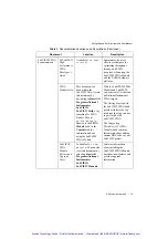
Note
The MGT_RefClk quad location and physical resource identify the physical
resource that clock signals use to enter the FPGA, but they still may act as a
Reference Clock for adjacent quads. Refer to the
Reference Clock Selection and
Distribution
section of
7 Series FPGAs GTX/GTH Transceivers User Guide
(UG476) for more information about cases when using single or multiple Reference
Clocks for single or multiple transceivers.
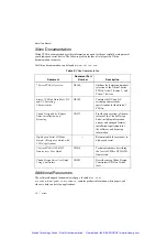
Signal Routing
The PXIe-6591R high-speed serial differential signals are routed directly from the Kintex-7
FPGA pins to the PORT 0 and PORT 1 connector pins using a 100 nF AC-coupling capacitor,
as shown in the following figure.
Figure 3-2.
PXIe-6591R Signal Routing
Socketed CLIP Interface
Socketed CLIP allows you to insert HDL IP into an FPGA target, enabling VHDL code to
communicate directly with an FPGA VI. Socketed CLIP also allows the CLIP to communicate
directly with circuitry external to the FPGA.
The following sections provide information about how to configure your device for use with
socketed CLIP.
Table 3-3.
Clock Signal and Quad Mapping
Clock Signal
Quad Location
Physical Resource
MGT_RefClk0
Quad 3 (Q3)
REFCLK1_Q3
MGT_RefClk1
Quad 2 (Q2)
REFCLK0_Q2
C
ab
le
100nF
Tx+
Rx+
Rx–
Tx–
100nF
Xilinx Kintex-7 FPGA
PORT 0 /
PORT 1
Connector
s
Artisan Technology Group - Quality Instrumentation ... Guaranteed | (888) 88-SOURCE | www.artisantg.com


