MOTOROLA
Chapter 1. Introduction
1-5
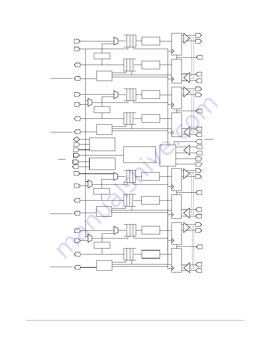
Block Diagram
Figure 1-2. MC92603 Block Diagram
8B10B
Encoder
8B10B
Decoder
Re
ce
ive
r
CLK GEN
XLINK_A_N
XLINK_A_P
RLINK_A_P
RLINK_A_N
T
ra
n
sm
itter
XMIT_A_[7:0]
RECV_A_[7:0]
RECV_A_RCLK
XMIT_A_K/ERR
PLL
LINK
Controller
REF_CLK_P
XMIT FIFO
RECV FIFO
BIST
8B10B
Encoder
8B10B
Decoder
Re
c
e
ive
r
CLK GEN
XLINK_B_N
XLINK_B_P
RLINK_B_P
RLINK_B_N
RECV_B_[7:0]
RECV_B_RCLK
XMIT_B_K/ERR
XMIT FIFO
RECV FIFO
XMIT_B_CLK
BIST
REF_CLK_N
8B10B
Encoder
8B10B
Decoder
CLK GEN
XLINK_C_N
XLINK_C_P
RLINK_C_P
RLINK_C_N
XMIT_C_[7:0]
XMIT_C_K/ERR
XMIT FIFO
RECV FIFO
XMIT_C_CLK
BIST
8B10B
Encoder
8B10B
Decoder
XLINK_D_N
XLINK_D_P
RLINK_D_P
RLINK_D_N
XMIT_D_[7:0]
XMIT_D_K/ERR
XMIT FIFO
RECV FIFO
BIST
Jtag
Controller
TDI,TRST,TCK
TMS
CLK GEN
XCVR_C_DISABLE
XCVR_D_DISABLE
XCVR_B_DISABLE
XCVR_A_DISABLE
XMIT_B_[7:0]
RECV_B_K
RECV_B_ERR
RESET
.
MDIO
Controller
MD_DATA
MD_ADR[4:2]
MD_CLK
RECV_B_RCLK
RECV_A_RCLK
RECV_B_DV
XMIT_A_CLK
MDIO_EN
XMIT_A_ENABLE
XMIT_B_ENABLE
XMIT_C_ENABLE
XMIT_D_ENABLE
XCVR_A_LBE
XCVR_B_LBE
XCVR_C_LBE
XCVR_D_LBE
GTX_CLK0
GTX_CLK1
TDO
RECV_B_COMMA
RECV_A_K
RECV_A_ERR
RECV_A_DV
RECV_A_COMMA
8B10B
Encoder
8B10B
Decoder
CLK GEN
LINK
REF_CLK_P
XMIT FIFO
RECV FIFO
BIST
8B10B
Encoder
8B10B
Decoder
CLK GEN
XMIT FIFO
RECV FIFO
BIST
8B10B
8B10B
Decoder
CLK GEN
XMIT FIFO
RECV FIFO
BIST
8B10B
Encoder
8B10B
Decoder
T
ran
smitte
r
RECV_D_[7:0]
RECV_D_RCLK
XMIT FIFO
RECV FIFO
XMIT_D_CLK
BIST
CLK GEN
Configuration Inputs
1
RECV_D_K
RECV_D_ERR
.
1
Configuration signal inputs are:
RECV_REF_A, COMPAT, REPE, HSE, ADIE, TBIE, BSYNC, LBOE, DROP_SYNC, TST_0, TST_1,
RECV_D_RCLK
RECV_D_DV
RECV_D_COMMA
WSYNC0, WSYNC1, STNDBY, XMIT_REF_A, MEDIA, RCCE, JPACK, RECV_CLK_CENT, DDR,
ENABLE_AN, USE_DIFF_CLK, ENAB_RED, BROADCAST, XCVR_A_RSEL, XCVR_B_RSEL
RECV_C_RCLK
RECV_C_ERR
RECV_C_[7:0]
RECV_C_K
RECV_C_RCLK
RECV_C_DV
RECV_C_COMMA
RECV_C_ERR
Re
c
e
ive
r
Re
c
e
iv
e
r
Re
ce
ive
r
T
ra
n
sm
itter
T
ran
sm
itt
e
r
TTL_REF_CLK
Summary of Contents for MC92603
Page 18: ...xviii MC92603 Quad Gigabit Ethernet Transceiver Reference Manual MOTOROLA ...
Page 26: ...1 8 MC92603 Quad Gigabit Ethernet Transceiver Reference Manual MOTOROLA References ...
Page 116: ...A 2 MC92603 Quad Gigabit Ethernet Transceiver Reference Manual MOTOROLA ...
Page 126: ...C 2 MC92603 Quad Gigabit Ethernet Transceiver Reference Manual MOTOROLA ...
Page 130: ...Glossary 4 MC92603 Quad Gigabit Ethernet Transceiver Reference Manual MOTOROLA ...