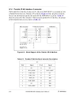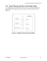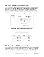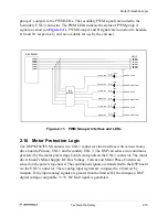
Zero-Crossing Detection
Technical Summary
2-23
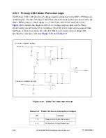
header pins, JG14, that allow the end user to select which signal group the DSP’s A/D will
monitor. Refer to
for the design of a single channel. The Secondary UNI-3’s
Back-EMF signals are simularly derived and routed to a group of header pins, JG10, that
allow the end user to select which signal group the DSP’s A/D will monitor, reference
Figure 2-15. Primary Back-EMF or Motor Phase Current Sense Signals
2.18 Quadrature Encoder/Hall-Effect Interface
The DSP56F807EVM board contains a Primary and Secondary Quadrature
Encoder/Hall-Effect interface connected to the DSP’s first and second Quad Encoder
input ports. The circuit is designed to 3.0V to +5.0V encoder or Hall-Effect sensor
inputs. Input noise filtering is supplied on the input path for the Quadrature
Encoder/Hall-Effect interface, along with additional noise rejection circuitry inside the
DSP.
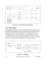
contains the primary encoder interface. The secondary encoder
interface is a duplicate of the primary encoder interface.
2.19 Zero-Crossing Detection
An attached UNI-3 motor drive board contains logic that can send out pulses when the
phase voltage of an attached 3-phase motor drops to zero. The motor drive board circuits
generate a 0 to +5.0V DC pulse via voltage comparators. The resulting pulse signals are
sent to a set of jumper blocks shared with the Encoder/Hall-Effect interface. The jumper
blocks allow the selection of Zero-Crossing signals or Quadrature Encoder/Hall-Effect
signals. When in operation, the DSP will only monitor one set of signals,
Encoder/Hall-Effect or Zero-Crossing.
contains the Zero-Crossing and
Encoder/Hall circuits.
Typical Motor Phase-Current/Back-EMF Analog Input Selector
BACK_EMF_A
PHASE_A_I_SENSE
1
2
3
AN2
JG14
Summary of Contents for Digital DNA DSP56F807
Page 2: ......
Page 12: ...xii DSP56F807EVM Hardware User s Manual ...
Page 53: ... DSP56F807EVM Schematics A 1 Appendix A DSP56F807EVM Schematics ...
Page 72: ...A 20 DSP56F807EVM Hardware User s Manual ...
Page 79: ......


