background image

Motor Protection Logic

Technical Summary

2-19

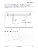
group A’s outputs to the PWM LEDs. The secondary PWM signals are routed to the 
Secondary UNI-3 connector. The PWM LEDs indicate the status of PWM group A 
signals, as shown in 

Figure 2-11

. PWM Group A and B signals are routed out to headers, 

J10 and J11 respectively, and are available for use by the end user.

Figure 2-11.   PWM Group A Interface and LEDs

2.16   Motor Protection Logic

The DSP56F807EVM contains two UNI-3 connectors that interface with various motor 
drive boards, Primary UNI-3 and Secondary UNI-3. The DSP can sense error conditions 
generated by the motor power stage boards via signals on the UNI-3 connector. The motor 
driver board’s Motor Supply DC Bus Voltage, Current and Motor Phase Currents are 
sensed on the power stage board. The conditioned signals are transferred to the DSP board 
via the UNI-3 connector. These analog input signals are compared to a limit set by 
trimpots. If the input analog signals are greater than the limit set by the trimpot, a DSP 
digital voltage-comp3.3V DC fault signal is generated.

DSP56F807

LED

BUFFER

UNI-3

PWMA0
PWMA1
PWMA2
PWMA3
PWMA4
PWMA5

PWMA0
PWMA1
PWMA2
PWMA3
PWMA4
PWMA5

YELLOW LED

GREEN LED

GREEN LED

GREEN LED

YELLOW LED

YELLOW LED

+3.3V

PHASE A TOP

PHASE A BOTTOM

PHASE B TOP

PHASE B BOTTOM

PHASE C TOP

PHASE C BOTTOM

LED4

LED5

LED6

LED7

LED8

LED9

Summary of Contents for Digital DNA DSP56F807

Page 1: ... Motorola Inc 2001 All rights reserved Semiconductor Products Sector DSP56F807 Evaluation Module Hardware User s Manual Order this document by DSP56F807EVMUM D Rev 0 02 2001 ...

Page 2: ......

Page 3: ...m and Data Memory 2 5 2 3 RS 232 Serial Communications 2 6 2 4 Clock Source 2 7 2 5 Operating Mode 2 7 2 6 Debug LEDs 2 8 2 7 Debug Support 2 8 2 7 1 JTAG Connector 2 9 2 7 2 Parallel JTAG Interface Connector 2 10 2 8 External Interrupts 2 11 2 9 Reset 2 12 2 10 Power Supply 2 13 2 11 Primary UNI 3 Interface 2 14 2 12 Secondary UNI 3 Interface 2 15 2 13 General Purpose Switches and Run Stop Switch...

Page 4: ...hannel A Expansion Connector 2 29 2 22 6 Secondary Encoder Timer Channel B Expansion Connector 2 29 2 22 7 Timer Channel C Expansion Connector 2 30 2 22 8 Timer Channel D Expansion Connector 2 30 2 22 9 Address Bus Expansion Connector 2 31 2 22 10 Data Bus Expansion Connector 2 32 2 22 11 A D Port A Expansion Connector 2 32 2 22 12 A D Port B Expansion Connector 2 33 2 22 13 Serial Communications ...

Page 5: ...2 12 2 8 Schematic Diagram of the Power Supply 2 13 2 9 Run Stop and General Purpose Switches 2 17 2 10 Serial 10 bit 4 Channel D A Converter 2 18 2 11 PWM Group A Interface and LEDs 2 19 2 12 FAULTA1 Selection Circuit 2 20 2 13 DC Bus Over Voltage and Phase Over Current Detection Circuits 2 21 2 14 FAULTB1 Selection Circuit 2 22 2 15 Primary Back EMF or Motor Phase Current Sense Signals 2 23 2 16...

Page 6: ...E ANALOG INPUT SELECTOR A 11 A 11 PRIMARY AND SECONDARY 3 PHASE OVER CURRENT SENSE A 12 A 12 PRIMARY ZERO CROSSING QUADRATURE ENCODER OR HALL EFFECT SELECTOR A 13 A 13 SECONDARY ZERO CROSSING QUADRATURE ENCODER OR HALL EFFECT SELECTOR A 14 A 14 DSP PORT EXPANSION CONNECTORS A 15 A 15 HIGH SPEED CAN INTERFACE A 16 A 16 PARALLEL JTAG HOST TARGET INTERFACE AND JTAG CONNECTOR A 17 A 17 POWER SUPPLIES ...

Page 7: ...1 CAN Header Description 2 25 2 12 Port B Connector Description 2 27 2 13 Port D Connector Description 2 27 2 14 Port E Connector Description 2 28 2 15 External Memory Control Signal Connector Description 2 28 2 16 Timer A Connector Description 2 29 2 17 Timer B Connector Description 2 29 2 18 Timer C Connector Description 2 30 2 19 Timer D Connector Description 2 30 2 20 External Memory Address B...

Page 8: ...viii DSP56F807EVM Hardware User s Manual 2 27 CAN Connector Description 2 34 2 28 PWM Port A Connector Description 2 35 2 29 PWM Port B Connector Description 2 35 ...

Page 9: ...ers and two appendixes Chapter 1 Introduction provides an overview of the EVM and its features Chapter 2 Technical Summary describes in detail the DSP56F807 hardware Appendix A DSP56F807EVM Schematics contains the schematics of the DSP56F807EVM Appendix B DSP56F807EVM Bill of Material provides a list of the materials used on the DSP56F807EVM board Suggested Reading More documentation on the DSP56F...

Page 10: ...alues Begin with a sym bol 0FF0 80 Decimal Values No special symbol attached to the number 10 34 Binary Values Begin with the letter b attached to the number b1010 b0011 Numbers Considered positive unless specifically noted as a negative value 5 10 Voltage is often shown as posi tive 3 3V Bold Reference sources paths emphasis see http www mot c om SPS DSP A D Analog to Digital CAN Controller Area ...

Page 11: ... debug LQFP Low profile Quad Flat Pack MPIO Multi Purpose Input and Output Port on Motorola s Family of DSPs Shares package pins with other peripherals on the chip and can function as a GPIO OnCETM On Chip Emulation a debug bus and port created by Motorola to enable designers to create a low cost hardware interface for a professional quality debug environment PCB Printed Circuit Board PLL Phase Lo...

Page 12: ...xii DSP56F807EVM Hardware User s Manual ...

Page 13: ...oard RAM run it and debug it using a debugger via the JTAG OnCETM port The breakpoint features of the OnCE port enable the user to easily specify complex break conditions and to execute user developed software at full speed until the break conditions are satisfied The ability to examine and modify all user accessible registers memory and peripherals through the OnCE port greatly facilitates the ta...

Page 14: ...G1 JG17 shown in Figure 1 2 are used to configure various features on the DSP56F807EVM board Table 1 1 describes the default jumper group settings DSP56F807 RESET MODE IRQ Address Data Control JTAG OnCE XTAL EXTAL SPI SCI 0 SCI 1 CAN TIMER GPIO PWM 1 A D 0 A D 1 PWM 2 3 3 V GND Peripheral Expansion Connector s RESET LOGIC MODE IRQ LOGIC Program Memory 64Kx16 bit SRAM Memory Expansion Connector s J...

Page 15: ...232 output NC JG10 Secondary UNI 3 3 Phase Current Sense Selected as inputs to A D 2 3 5 6 8 9 JG11 Secondary UNI 3 serial selected 1 2 3 4 5 6 7 8 JG12 Primary Encoder Input Selected 2 3 5 6 8 9 JG13 Secondary Encoder Input Selected 2 3 5 6 8 9 JG14 Primary UNI 3 3 Phase Current Sense Selected as inputs to A D 2 3 5 6 8 9 JG15 Primary UNI 3 serial selected 1 2 3 4 5 6 7 8 JG16 PD0 input selected ...

Page 16: ...P56F807EVM board This provides the connection which allows the host computer to control the board 3 Make sure that the external 12V DC 4 0A power supply is not plugged into a 120V AC power source 4 Connect the 2 1mm output power plug from the external power supply into P2 shown in Figure 1 3 on the DSP56F807EVM board 5 Apply power to the external power supply The green Power On LED LED10 will illu...

Page 17: ...well as for learning the architecture and instruction set of the DSP56F807 processor The main features of the DSP56F807EVM with board and schematic reference designators include DSP56F807 16 bit 3 3V Digital Signal Processor operating at 80MHz U1 External fast static RAM FSRAM memory U2 configured as 64K 16 bit of program memory with 0 wait states at 70MHz 64K 16 bit of data memory with 0 wait sta...

Page 18: ...r own Timer B MPIO compatible peripheral J21 Connector to allow the user to connect their own Timer C MPIO compatible peripheral J19 Connector to allow the user to connect their own Timer D MPIO compatible peripheral J22 Connector to allow the user to attach their own Port B GPIO compatible peripheral J20 Connector to allow the user to attach their own Port D GPIO compatible peripheral J23 Connect...

Page 19: ...rrent sensing U6 Phase Current sensing U5 and U6 Back EMF sensing and selector JG10 Temperature sensing Zero Crossing detection and selector JG10 Pulse Width Modulation Manual RESET push button S1 Manual interrupt push button for IRQA S2 Manual interrupt push button for IRQB S3 General purpose push button on GPIO PD3 S4 General purpose push button on GPIO PD4 S5 General purpose toggle switch for R...

Page 20: ...n overview description of the DSP and detailed information about the on chip components including the memory and I O maps peripheral functionality and control status register descriptions for each subsystem DSP56F80x Family Manual DSP56F80xFM AD Provides a detailed description of the core processor including internal status and control registers and a detailed description of the family instruction...

Page 21: ...ry chip s A0 signal line half of the memory chip is selected when program memory accesses are requested and the other half of the memory chip is selected when data memory access are requested This memory bank will operate with zero wait state accesses while the DSP56F807 is running at 70MHz However when running at 80MHz the memory bank operates with four wait state accesses This memory bank can be...

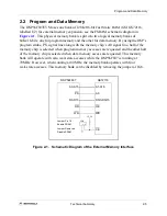
Page 22: ...ow control is not provided but could be implemented using uncommitted GPIO signals The pinout of connector P3 is listed in Table 2 1 The RS 232 level converter transceiver can be disabled by placing a jumper at JG9 Figure 2 2 Schematic Diagram of the RS 232 Interface Table 2 1 RS 232 Serial Connector Description P3 Pin Signal Pin Signal 1 Jumper to 6 4 6 Jumper to 1 4 2 TXD 7 Jumper to 8 3 RXD 8 J...

Page 23: ...3 Figure 2 3 Schematic Diagram of the Clock Interface 2 5 Operating Mode The DSP56F807EVM provides a boot up MODE selection jumper JG7 This jumper is used to select the operating mode of the DSP as it exits RESET Refer to the DSP56F807 User s Manual for a complete description of the chip s operating modes Table 2 2 shows the two operation modes available on the DSP56F807 Table 2 2 Operating Mode S...

Page 24: ...ser LED3 is controlled by PB2 Setting PB0 PB1 or PB2 to a Logic One value will turn on the associated LED Figure 2 4 Schematic Diagram of the Debug LED Interface 2 7 Debug Support The DSP56F807EVM provides an on board Parallel JTAG Host Target Interface and a JTAG interface connector for external Target Interface support Two interface connectors are provided to support each of these debugging appr...

Page 25: ...ger program Table 2 3 shows the pin out for this connector When this connector is used with an external Host Target Interface the parallel JTAG interface should be disabled by placing a jumper in jumper block JG4 Reference Table 2 4 for this jumper s selection options Table 2 3 JTAG Connector Description J3 Pin Signal Pin Signal 1 TDI 2 GND 3 TDO 4 GND 5 TCK 6 GND 7 NC 8 KEY 9 RESET 10 TMS 11 3 3V...

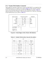
Page 26: ...allel JTAG interface the jumper at JG4 should be removed as shown in Table 2 4 Figure 2 5 Block Diagram of the Parallel JTAG Interface Table 2 5 Parallel JTAG Interface Connector Description P1 Pin Signal Pin Signal 1 NC 14 NC 2 PORT_RESET 15 PORT_IDENT 3 PORT_TMS 16 NC 4 PORT_TCK 17 NC 5 PORT_TDI 18 GND 6 PORT_TRST 19 GND 7 NC 20 GND 8 PORT_IDENT 21 GND DB 25 Connector Parallel JTAG Interface DSP...

Page 27: ...QA S3 allows the user to generate a hardware interrupt for signal line IRQB These two switches allow the user to generate interrupts for his user specific programs Figure 2 6 Schematic Diagram of the User Interrupt Interface 9 PORT_VCC 22 GND 10 NC 23 GND 11 PORT_TDO 24 GND 12 NC 25 GND 13 PORT_CONNECT Table 2 5 Parallel JTAG Interface Connector Description P1 Pin Signal Pin Signal DSP56F807 IRQA ...

Page 28: ... a clean Power On RESET signal Additional reset logic is provided to support the RESET signals from the JTAG connector the Parallel JTAG Interface and the user RESET push button refer to Figure 2 7 Figure 2 7 Schematic Diagram of the RESET Interface RESET PUSHBUTTON MANUAL RESET P_RESET RESET 3 3V ...

Page 29: ...user motor control applications when connected to an optional motor power stage board The DSP56F807EVM provides 3 3V DC voltage regulation for the DSP memory D A CAN parallel JTAG interface and supporting logic refer to Figure 2 8 Power applied to the DSP56F807EVM is indicated with a Power On LED referenced as LED10 Figure 2 8 Schematic Diagram of the Power Supply 12V DC 5 0V Regulator POWER ON GR...

Page 30: ...ent signals Refer to Table 2 6 for the pin out of the Primary UNI 3 connector J1 Table 2 6 Primary UNI 3 Connector Description J1 Pin Signal Pin Signal 1 PWM_AT 2 Shield 3 PWM_AB 4 Shield 5 PWM_BT 6 Shield 7 PWM_BB 8 Shield 9 PWM_CT 10 Shield 11 PWM_CB 12 GND 13 GND 14 5 0V DC 15 5 0V DC 16 Analog 3 3V DC 17 Analog GND 18 Analog GND 19 Analog 15V DC 20 Analog 15V DC 21 Motor DC Bus Voltage Sense 2...

Page 31: ...WM Port B The header JG10 is used to select between the Back EMF and Motor Phase Current signals Refer to Table 2 7 for the pin out of the Secondary UNI 3 connector J2 37 Shield 38 Back EMF Phase A Sense 39 Back EMF Phase B Sense 40 Back EMF Phase C Sense Table 2 7 Secondary UNI 3 Connector Description J2 Pin Signal Pin Signal 1 PWM_AT 2 Shield 3 PWM_AB 4 Shield 5 PWM_BT 6 Shield 7 PWM_BB 8 Shield...

Page 32: ...8 Shield 29 Motor Drive Brake Control 30 Serial COM 31 PFC PWM 32 PFC Inhibit 33 PFC Zero Cross 34 Zero Cross A 35 Zero Cross B 36 Zero Cross C 37 Shield 38 Back EMF Phase A Sense 39 Back EMF Phase B Sense 40 Back EMF Phase C Sense Table 2 7 Secondary UNI 3 Connector Description Continued J2 Pin Signal Pin Signal ...

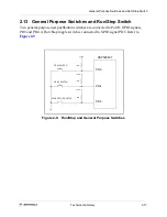
Page 33: ...itch Two general purpose user pushbutton switches are connected to Port D GPIO signals PD3 and PD4 A Run Stop toggle switch is connected to GPIO signal PD5 Refer to Figure 2 9 Figure 2 9 Run Stop and General Purpose Switches DSP56F807 3 3V PD3 PD4 PD5 3 3V 10K 10K 10K GP 1 SWITCH GP 2 SWITCH START STOP SWITCH 3 3V ...

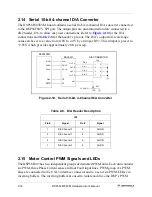
Page 34: ...er step Figure 2 10 Serial 10 bit 4 Channel D A Converter 2 15 Motor Control PWM Signals and LEDs The DSP56F807 has two independent groups of dedicated PWM units Each unit contains six PWM three Phase Current sense and four Fault input lines PWM group A s PWM lines are connected to the UNI 3 interface connector and to a set of six PWM LEDs via inverting buffers The inverting buffers are used to is...

Page 35: ...onditions generated by the motor power stage boards via signals on the UNI 3 connector The motor driver board s Motor Supply DC Bus Voltage Current and Motor Phase Currents are sensed on the power stage board The conditioned signals are transferred to the DSP board via the UNI 3 connector These analog input signals are compared to a limit set by trimpots If the input analog signals are greater tha...

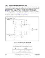
Page 36: ...f the Over Voltage and one phase of the Phase Over Current circuit for the UNI 3 interface The FAULTA1 input can be sourced from the Phase A Over Current circuit or the DC Bus Over Current circuit Jumper JG1 provides the selection reference Figure 2 12 and Table 2 9 Figure 2 12 FAULTA1 Selection Circuit Table 2 9 FAULTA1 Source Selection Jumper JG1 Comment 1 2 Phase A Over Current Sense input 2 3 ...

Page 37: ... to the DSP s PWM group B fault inputs i e FAULTB1 FAULTB2 and FAULTB3 The Secondary UNI 3 interface is similar to the circuits contained in Figure 2 13 The FAULTB1 input can be sourced from the Phase A Over Current circuit or the DC Bus Over Current circuit Jumper JG16 provides the selection reference Figure 2 14 and Table 2 10 Figure 2 13 DC Bus Over Voltage and Phase Over Current Detection Circ...

Page 38: ...d from a resistor divider network contained in the motor drive unit These resistors divide down the attached motor s Back EMF voltages to a 0 to 3 3V level The Motor Phase Current signals are derived from current sense resistors Both of these signal groups are then routed to a group of Table 2 10 FAULTB1 Source Selection Jumper JG2 Comment 1 2 Phase A Over Current Sense input 2 3 DC Bus Over Curre...

Page 39: ...on the input path for the Quadrature Encoder Hall Effect interface along with additional noise rejection circuitry inside the DSP Figure 2 16 contains the primary encoder interface The secondary encoder interface is a duplicate of the primary encoder interface 2 19 Zero Crossing Detection An attached UNI 3 motor drive board contains logic that can send out pulses when the phase voltage of an attac...

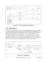
Page 40: ...or are provided to allow easy daisy chaining of CAN devices CAN bus termination of 120 ohms can be provided by adding a jumper to JG3 Refer to Table 2 11 for the CAN connector signals and to Figure 2 17 for a connection diagram Figure 2 17 CAN Interface ZERO_X_A ZERO_X_B ZERO_X_C 1 2 3 4 5 6 5 0V FILTER FILTER FILTER FILTER PIN 1 5 0V PIN 2 GROUND PIN 3 PHASE A PIN 4 PHASE B PIN 5 INDEX PIN 6 HOME...

Page 41: ...ort pins PD0 and PD1 are pulled high with 10K ohm resistors on JG16 and JG17 Attaching a jumper will ground the respective port D signal line see Figure 2 18 Figure 2 18 Software Feature Jumpers Table 2 11 CAN Header Description J24 and J25 Pin Signal Pin Signal 1 NC 2 NC 3 CANL 4 CANH 5 GND 6 NC 7 NC 8 NC 9 NC 10 NC DSP56F807 PD0 PD1 JG16 JG17 1 2 3 1 2 3 10K 10K 10K 10K 3 3V 3 3V User Jumper 0 U...

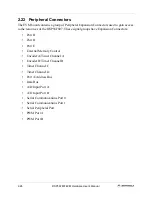
Page 42: ...sources of the DSP56F807 These signal groups have Expansion Connectors Port B Port D Port E External Memory Control Encoder A Timer Channel A Encoder B Timer Channel B Timer Channel C Timer Channel D Port A Address Bus Data Bus A D Input Port A A D Input Port B Serial Communications Port 0 Serial Communications Port 1 Serial Peripheral Port PWM Port A PWM Port B ...

Page 43: ...sion Connector Port D is an MPIO port with signal lines attached to various headers The six pins of the port PD0 PD5 are dedicated to general purpose operation The remaining two pins PD6 and PD7 are shared with the TXD1 and RXD1 signal lines The GPIO port pins may be programmed as inputs outputs or level sensitive interrupt inputs Table 2 13 shows the exclusive Port D signals The shared Port D sig...

Page 44: ...sion Connector The External Memory Control Signal connector contains the DSP s external memory control signal lines Refer to Table 2 15 for the names of these signals Table 2 14 Port E Connector Description J17 Pin Signal Alternate Funct Pin Signal Alternate Funct 1 PE0 TXD0 2 PE1 RXD0 3 PE2 TXD1 4 PE3 RXD1 5 PE4 SCLK 6 PE5 MOSI 7 PE6 MISO 8 PE7 SS 9 GND GND 10 3 3V 3 3V Table 2 15 External Memory...

Page 45: ...er Timer Channel B Expansion Connector The Secondary Encoder Timer Channel B port is an MPIO port attached to the Timer B expansion connector The port can act as a Quadrature Decoder interface port or as a general purpose Timer port Refer to Table 2 17 for the signals attached to the connector Table 2 16 Timer A Connector Description J18 Pin Signal Alternate 1 TA0 PhaseA0 2 TA1 PhaseB0 3 TA2 INDEX...

Page 46: ... signals attached to the connector 2 22 8 Timer Channel D Expansion Connector The Timer Channel D port is an MPIO port attached to the Timer D expansion connector Refer to Table 2 19 for the signals attached to the connector Table 2 18 Timer C Connector Description J19 Pin Signal 1 TC0 2 TC1 3 3 3V 4 GND Table 2 19 Timer D Connector Description J22 Pin Signal 1 TD0 2 TD1 3 TD2 4 TD3 5 3 3V 6 GND ...

Page 47: ...al memory address signal lines The upper 8 bits A8 A15 can also be used as Port A GPIO lines See Table 2 20 for the Address bus connector information Table 2 20 External Memory Address Bus Connector Description J6 Pin Signal Pin Signal 1 A0 2 A1 3 A2 4 A3 5 A4 6 A5 7 A6 8 A7 9 A8 10 A9 11 A10 12 A11 13 A12 14 A13 15 A14 16 A15 17 GND 18 3 3V ...

Page 48: ...tor The 8 channel Analog to Digital conversion port A is attached to this connector See Table 2 22 for the connection information Table 2 21 External Memory Address Bus Connector Description J7 Pin Signal Pin Signal 1 D0 2 D1 3 D2 4 D3 5 D4 6 D5 7 D6 8 D7 9 D8 10 D9 11 D10 12 D11 13 D12 14 D13 15 D14 16 D15 17 GND 18 3 3V Table 2 22 A D Port A Connector Description J9 Pin Signal Pin Signal 1 AN0 2...

Page 49: ...tion information 2 22 13 Serial Communications Port 0 Expansion Connector The Serial Communications Port 0 SCI0 is attached to this connector See Table 2 24 for the connection information Table 2 23 A D Port B Connector Description J12 Pin Signal Pin Signal 1 AN8 2 AN12 3 AN9 4 AN13 5 AN10 6 AN14 7 AN11 8 AN15 9 GNDA 10 3 3VA Table 2 24 SCI0 Connector Description J15 Pin Signal 1 TXD0 2 RXD0 3 GND...

Page 50: ...or The Serial Peripheral Interface SPI is attached to this connector Refer to Table 2 26 for the connection information 2 22 16 CAN Expansion Connector The CAN port is attached to this connector See Table 2 27 for the connection information Table 2 25 SCI1 Connector Description J14 Pin Signal 1 TXD1 2 RXD1 3 GND Table 2 26 SPI Connector Description J13 Pin Signal 1 MOSI 2 MISO 3 SCLK 4 GND Table 2...

Page 51: ...to this connector Refer to Table 2 29 for the connection information Table 2 28 PWM Port A Connector Description J10 Pin Signal Pin Signal 1 PWMA0 2 PWMA1 3 PWMA2 4 PWMA3 5 PWMA4 6 PWMA5 7 FAULTA0 8 FAULTA1 9 FAULTA2 10 FAULTA3 11 ISA0 12 ISA1 13 ISA2 14 GND Table 2 29 PWM Port B Connector Description J11 Pin Signal Pin Signal 1 PWMB0 2 PWMB1 3 PWMB2 4 PWMB3 5 PWMB4 6 PWMB5 7 FAULTB0 8 FAULTB1 9 F...

Page 52: ... board has a total of eight test points Four test points are located near the breadboard area 3 3VA AGND 3 3V and GND Three test points are located near the Primary UNI 3 connector J1 15VA GND and 15VA The final test point GND is located in the upper left corner of the board ...

Page 53: ... DSP56F807EVM Schematics A 1 Appendix A DSP56F807EVM Schematics ...

Page 54: ... TRST TDO TDI TMS TCK PS DS WR RD IRQA IRQB EXTBOOT CLKO EXTAL XTAL RESET RSTO TC0 TC1 TD1 TD0 TD3 TD2 TXD1 RXD1 RXD0 TXD0 PB0 PB1 PB2 PB3 PB4 PB6 PB7 PB5 PD2 PD3 PD4 PD5 PD0 PD1 PWMA1 PWMA2 PWMA5 ISA1 ISA0 ISA2 FAULTA0 FAULTA3 FAULTA1 FAULTA2 PWMA0 PWMA4 PWMA3 PHASEA0 HOME0 INDEX0 PHASEB0 PWMB1 PWMB2 PWMB3 PWMB5 ISB1 ISB2 FAULTB0 FAULTB3 FAULTB1 FAULTB2 PWMB4 PWMB0 ISB0 AN6 AN0 AN7 AN2 AN1 AN5 AN...

Page 55: ...esign RESET MODE CLOCK IRQS 63A10516S 1 0 2 18 Monday October 16 2000 A DSP Standard Products Division 2100 East Elliot Road Tempe Arizona 85284 Title Document Date Size Designer Sheet of Rev Number 480 413 5090 FAX 480 413 2510 POR POR IRQA IRQB EXTBOOT EXTAL XTAL 3 3V 3 3V 3 3V 3 3V 3 3V JG5 1 2 3 Y1 8 00MHz S1 S2 S3 R84 10K R83 10K R82 10K R1 10M JG7 1 2 JG6 1 2 U17 DS1818 DNP 2 1 3 Vcc RST GND...

Page 56: ...Arizona 85284 Title Document Date Size Designer Sheet of Rev Number 480 413 5090 FAX 480 413 2510 D2 D5 D13 D4 D0 D6 D15 D11 D3 D10 D1 D7 D12 D9 D8 D14 A15 A11 A1 A12 A10 A3 A14 A5 A9 A6 A8 A0 A7 A13 A2 A4 RD WR D 0 15 A 0 15 PS 3 3V 3 3V U2 GS72116TP 12 7 8 1 9 10 2 13 14 3 15 16 4 29 30 5 31 32 18 35 36 19 37 38 20 21 24 25 26 27 42 43 44 40 39 41 17 6 22 34 12 33 11 DQ1 DQ2 A4 DQ3 DQ4 A3 DQ5 DQ...

Page 57: ...Document Date Size Designer Sheet of Rev Number 480 413 5090 FAX 480 413 2510 R4IN R5IN R2IN R3IN T3IN EN T2IN T2IN T3IN EN R3IN R4IN R5IN R2IN TXD0 RXD0 3 3V 3 3V 3 3V R94 1K R95 1K R93 1K R92 1K R89 1K R91 1K R88 1K C60 1 0uF C61 1 0uF C63 1 0uF C62 1 0uF JG9 1 2 R90 1K T14 1 T15 1 T16 1 T17 1 P3 5 9 4 8 3 7 2 6 1 T13 1 T12 1 T22 1 T21 1 U13 MAX3245EEAI 27 1 26 2 23 28 14 13 12 19 18 17 16 15 8 ...

Page 58: ...2000 A DSP Standard Products Division 2100 East Elliot Road Tempe Arizona 85284 Title Document Date Size Designer Sheet of Rev Number 480 413 5090 FAX 480 413 2510 D A3 D A2 D A1 D A0 Vref MISO SCLK MOSI PB4 RSTO 3 3V 3 3V 3 3VA Vref R96 5 1K U14 MAX5251BEAP 1 2 3 4 5 6 15 16 17 18 19 20 13 9 12 10 8 7 14 11 AGND FBA OUTA OUTB FBB REFAB REFCD FBC OUTC OUTD FBD VDD UP0 DIN DOUT SCLK CS CL PDL DGND ...

Page 59: ...2000 A DSP Standard Products Division 2100 East Elliot Road Tempe Arizona 85284 Title Document Date Size Designer Sheet of Rev Number 480 413 5090 FAX 480 413 2510 PWMA4 PWMA1 PWMA0 PWMA5 PWMA2 PWMA3 PB0 PB1 PB2 3 3V 3 3V R98 270 R99 270 R100 270 R101 270 R102 270 R103 270 R104 270 R105 270 R106 270 U15A 74AC04 1 2 U15B 74AC04 3 4 U15C 74AC04 5 6 U15D 74AC04 9 8 U15E 74AC04 11 10 U15F 74AC04 13 12...

Page 60: ... PHASE C ZERO CROSSING PHASE A ZERO CROSSING PHASE B ZERO CROSSING DSPD Design PRIMARY UNI 3 INTERFACE AND OVER VOLTAGE FAULT DETECTION 63A10516S 1 0 7 18 Tuesday October 24 2000 B DSP Standard Products Division 2100 East Elliot Road Tempe Arizona 85284 Title Document Date Size Designer Sheet of Rev Number 480 413 5090 FAX 480 413 2510 GND GND GNDA GNDA PFC_PWM PFC_ZERO_CROSS SERIAL_COMM PFC_INHIB...

Page 61: ...NDARY UNI 3 OVER VOLTAGE SENSE SU3_V_S_DCB DSPD Design SECONDARY UNI 3 AND OVER VOLTAGE FAULT DETECTION 63A10516S 1 0 8 18 Tuesday October 24 2000 B DSP Standard Products Division 2100 East Elliot Road Tempe Arizona 85284 Title Document Date Size Designer Sheet of Rev Number 480 413 5090 FAX 480 413 2510 GND GND GNDA GNDA SU3_PFC_PWM SU3_PFC_ZERO_CROSS SU3_SERIAL_COMM SU3_PFC_INHIBIT SU3_PFC_ZERO_...

Page 62: ...ser 0 Jumper User 1 DSPD Design USER GENERAL PURPOSE SWITCHES AND JUMPERS 63A10516S 1 0 9 18 Monday October 16 2000 A DSP Standard Products Division 2100 East Elliot Road Tempe Arizona 85284 Title Document Date Size Designer Sheet of Rev Number 480 413 5090 FAX 480 413 2510 PD3 PD4 PD5 PD3 PD4 PD5 PD0 PD1 3 3V 3 3V 3 3V R120 10K S4 S5 JG16 1 2 3 R122 10K R121 10K JG17 1 2 3 R123 10K R117 10K R118 ...

Page 63: ... 8 9 7 JG10 DSPD Design MOTOR PHASE CURRENT BACK EMF VOLTAGE ANALOG INPUT SELECTOR 63A10516S 1 0 10 18 Monday October 16 2000 A DSP Standard Products Division 2100 East Elliot Road Tempe Arizona 85284 Title Document Date Size Designer Sheet of Rev Number 480 413 5090 FAX 480 413 2510 BK_EMF_B BK_EMF_C U3_PHA_IS AN2 U3_PHB_IS AN3 U3_PHC_IS AN4 BK_EMF_A SU3_PHA_IS AN10 AN11 AN12 SU3_BK_EMF_A SU3_PHB...

Page 64: ... Title Document Date Size Designer Sheet of Rev Number 480 413 5090 FAX 480 413 2510 S_PHA_IS PRI_OVER_I_LIMIT P_PHA_IS U3_I_LIMIT_REF U3_I_LIMIT_REF U3_I_LIMIT_REF SU3_I_LIMIT_REF SU3_I_LIMIT_REF SU3_I_LIMIT_REF P_PHA_IS P_OI_FAULT SEC_OVER_I_LIMIT S_PHA_IS S_OI_FAULT FAULTA3 FAULTA2 FAULTB3 FAULTB2 AN1 FAULTA1 U3_PHA_IS U3_PHB_IS U3_PHC_IS SU3_PHA_IS SU3_PHB_IS SU3_PHC_IS AN9 FAULTB1 3 3V 3 3V 3...

Page 65: ...OSSING QUADRATURE ENCODER OR HALL EFFECT SELECTOR 63A10516S 1 0 12 18 Monday October 16 2000 A DSP Standard Products Division 2100 East Elliot Road Tempe Arizona 85284 Title Document Date Size Designer Sheet of Rev Number 480 413 5090 FAX 480 413 2510 HOME0 ZERO_X_C ZERO_X_B ZERO_X_A INDEX0 PHASEB0 PHASEA0 5 0V 5 0V 5 0V 5 0V 5 0V R49 24 Ohm C22 470pF R48 24 Ohm R47 1K R46 24 Ohm R45 24 Ohm R44 1K...

Page 66: ...DARY ZERO CROSSING QUADRATURE ENCODER OR HALL EFFECT SELECTOR 63A10516S 1 0 13 18 Monday October 16 2000 A DSP Standard Products Division 2100 East Elliot Road Tempe Arizona 85284 Title Document Date Size Designer Sheet of Rev Number 480 413 5090 FAX 480 413 2510 HOME1 SU3_ZERO_X_C SU3_ZERO_X_B SU3_ZERO_X_A PHASEA1 PHASEB1 INDEX1 5 0V 5 0V 5 0V 5 0V 5 0V R58 24 Ohm R57 24 Ohm R56 1K C27 470pF R55 ...

Page 67: ...STO IRQB RESET IRQA WR RD PS RXD1 SS TXD0 RXD0 SCLK MISO MOSI TXD1 CLKO TD3 TD2 TD1 TC0 TC1 DEBUG_EVENT PHASEA1 PHASEB1 INDEX1 HOME1 TD0 PHASEA0 PHASEB0 INDEX0 HOME0 AN0 AN1 AN2 AN3 AN4 AN5 AN6 AN7 A 0 15 A 0 15 D 0 15 D 0 15 MOSI MISO SCLK TXD1 RXD1 TXD0 RXD0 MSCAN_TX MSCAN_RX AN8 AN9 AN10 AN11 AN12 AN13 AN14 AN15 PWMB0 PWMB2 PWMB4 PWMB1 PWMB3 PWMB5 FAULTB0 FAULTB2 FAULTB1 FAULTB3 ISB0 ISB2 ISB1 ...

Page 68: ...FACE 63A10516S 1 0 15 18 Monday October 16 2000 A DSP Standard Products Division 2100 East Elliot Road Tempe Arizona 85284 Title Document Date Size Designer Sheet of Rev Number 480 413 5090 FAX 480 413 2510 CANH CANL CANH CANL CANH CANL MSCAN_TX MSCAN_RX 5 0V 5 0V J24 1 3 5 7 9 2 4 6 8 10 U8 PCA82C250T 1 4 2 3 5 6 7 8 TXD RXD GND VCC VREF CANL CANH SLOPE R62 1K J25 1 3 5 7 9 2 4 6 8 10 JG3 1 2 R63...

Page 69: ... P_RESET J_TRST J_RESET TDO P_RESET TMS TCK TDI J_TRST TDO PORT_TDO PORT_TMS PORT_TRST PORT_TCK PORT_TDI PORT_CONNECT PORT_RESET PORT_IDENT J_TRST J_RESET J_TRST J_RESET TDI TDO TCK TMS RESET TRST POR 3 3V 3 3V 3 3V 3 3V 3 3V R70 51 Ohm R75 5 1K R73 5 1K J3 1 3 5 7 9 11 13 2 4 6 8 10 12 14 R77 47K R76 47K R64 270 R66 270 R65 270 R68 270 R67 270 R72 5 1K JG4 1 2 U9 MC74LCX244DW 18 16 14 12 9 7 5 3 ...

Page 70: ...8 Monday October 16 2000 B DSP Standard Products Division 2100 East Elliot Road Tempe Arizona 85284 Title Document Date Size Designer Sheet of Rev Number 480 413 5090 FAX 480 413 2510 5 0V 3 3V 3 3V 3 3VA 5 0V 5 0V_UNI3 3 3VA 3 3V VCC R78 470 P2 1 3 2 C29 0 1uF C30 0 1uF U11 MC33269DT 3 3 3 2 4 1 VIN VOUT VOUT GND U10 MC33269DT 5 0 3 2 4 1 VIN VOUT VOUT GND L1 FERRITE BEAD L3 FERRITE BEAD L2 FERRI...

Page 71: ...ion 2100 East Elliot Road Tempe Arizona 85284 Title Document Date Size Designer Sheet of Rev Number 480 413 5090 FAX 480 413 2510 3 3V 3 3V 5 0V 3 3V Vref 3 3V 3 3VA 3 3V 3 3V 3 3V 3 3VA 3 3V 3 3V 5 0V 5 0V 5 0V 5 0V 5 0V 3 3V 3 3V C56 0 1uF C55 0 01uF C46 0 01uF C50 0 1uF C48 0 1uF C54 0 1uF C51 0 1uF C52 0 1uF R79 5 1k C53 0 01uF C36 0 01uF C40 0 1uF C45 0 1uF C44 0 01uF C49 0 01uF C41 0 1uF C35...

Page 72: ...A 20 DSP56F807EVM Hardware User s Manual ...

Page 73: ... 3 3 U11 ON Semiconductor MC33269DT 3 3 1 GS72116 U2 GSI GS72116TP 12 1 MAX3245 U13 Maxim MAX3245EEAI 1 MAX5251 U14 Maxim MAX5251BEAP 1 PCA82C250T U8 Philips Semiconductor PCA82C250T 1 74AC00 U18 Fairchild 74AC00SC Resistors 20 16K Ω R8 R11 R16 R19 R24 R29 R31 R32 R107 R108 R112 R113 SMEC RC73L2A16KOHMJT 10 1M Ω R4 R5 R12 R13 R20 R21 R30 R33 R109 R114 SMEC RC73L2A1MOHMJT 18 5 1K Ω R6 R7 R14 R15 R2...

Page 74: ...R39 R40 R42 R43 R45 R46 R48 R49 R51 R52 R54 R55 R57 R58 R60 R61 SMEC RC73L2A24OHMJT 1 120 Ω 1 4W R63 YAGEO CFR 120QBK Potentioneters 7 10K Ω R2 R3 R36 R37 R97 R111 R116 BC MEPCOPAL ST4B103CT Inductors 4 1 0mH L1 L2 L3 L4 Panasonic EXC ELSA35V LEDs 1 Red LED LED1 Hewlett Packard HSMS C650 4 Yellow LED LED2 LED4 LED6 LED8 Hewlett Packard HSMY C650 5 Green LED LED3 LED5 LED7 LED9 LED10 Hewlett Packar...

Page 75: ...stick JG1 JG2 JG5 J14 J15 JG16 J16 JG17 SAMTEC TSW 103 07 S S 4 4 2 Bergstick JG11 JG15 J23 J26 SAMTEC TSW 104 07 S D 6 1 2 Bergstick JG3 JG4 JG6 JG7 JG8 JG9 SAMTEC TSW 102 07 S S 4 3 x 3 Bergstick JG10 JG12 JG13 JG14 SAMTEC TSW 103 07 S T 2 9 x 2 Bergstick J6 J7 SAMTEC TSW 109 07 S D 3 6 x 1 Bergstick J18 J21 J22 SAMTEC TSW 106 07 S S 6 5 x 2 Bergstick J9 J12 J17 J20 J24 J25 SAMTEC TSW 105 07 S D...

Page 76: ...HENOL 617 C025P AJ121 1 2 1mm coax Power Connector P2 Switch Craft RAPC 722 1 DE9F Connector P3 AMPHENOL 617 C009S AJ120 Switches 5 SPST Pushbutton S1 S5 Panasonic EVQ PAD05R 1 SPDT Toggle S6 C K GT11MSCKE Transistors 1 2N2222A Q1 ZETEX FMMT2222ACT Miscellaneous 28 Shunt SH1 SH28 Samtec SNT 100 BL T 6 Rubber Feet RF1 RF6 3M SJ5018BLKC Qty Description Ref Designators Vendor Part ...

Page 77: ...ermination 2 1 CAN bypass 2 1 CAN interface 2 1 CAN physical layer peripheral 2 2 Development Card 2 1 external memory expansion connectors 2 2 external oscillator frequency input 2 1 FSRAM 2 1 JTAG port interface 2 1 MPIO compatible peripheral 2 2 On board power regulation 2 2 Parallel JTAG Host Target Interface 2 1 PWM compatible peripheral 2 2 real time debugging 2 8 RS 232 interface 2 1 SPI co...

Page 78: ...Operating Mode 2 7 P PCB xi Peripheral Connectors 2 26 PLL xi Program memory 2 5 PWM xi Q Quad Encoder 2 23 Quadrature Decoder interface port 2 29 Quadrature Encoder Hall Effect interface 2 23 R RAM xi ROM xi RS 232 interface 2 6 level converter 2 6 schematic diagram 2 6 RS 232 Serial Communications 2 6 S SCI xi Serial Communications Port 2 33 2 34 SPI xi Serial Peripheral Interface 2 34 SRAM xi e...

Page 79: ......
Page 80: ...se Motorola products for any such unintended or unauthorized application Buyer shall indemnify and hold Motorola and its officers employees subsidiaries affiliates and distributors harmless against all claims costs damages and expenses and reasonable attorney fees arising out of directly or indirectly any claim of personal injury or death associated with such unintended or unauthorized use even if...

Reviews: