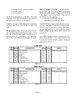


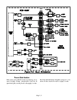
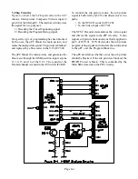


Page 4-7
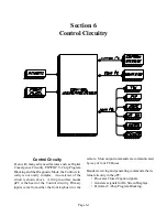
Convergence Control Circuitry
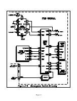
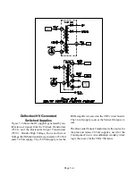
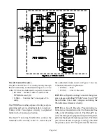
Figure 4-6 illustrates the Convergence Control Cir-
cuitry. The Main Control Microprocessor, IC700,
controls the Convergence circuit over the CSDA se-
rial data line. Transfer of data is timed by CSCL
clock signal from IC700.
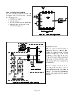
The ACK line informs the Microprocessor (uPC) that
IC800 has received a response from the E
2
PROM.
If an expected response is not received, IC800 pulls
the ACK LOW, telling the uPC that the response is
missing. When this occurs, the uPC will repeat the
initial command.
The C_BUSY line informs the uPC if IC800 is busy,
performing a command, or communicating with the
E
2
PROM. When IC800 is busy, it pulls the C_BUSY
line LOW. If the line remains LOW for an extended
period of time, the uPC assumes the Convergence
circuitry is locked up and initiates a Reset command.
A LOW on the NOT E2RESET line, from pin 20 of
IC700, will set all convergence data to its nominal
point.
Convergence data is stored, and read in IC801, an
E
2
PROM. Data is written, and read from memory
over the SDAM line, and timed by the SCLK line.
PLL circuitry in IC809 generates timing signals for
the operation of IC800, and the generation of the
internal Crosshatch pattern. The PLL is phase locked
to horizontal sync, input to IC809 at pin 4.
IC800 also outputs two clock signals, BCLK at pin
28, and WCLK at pin 27. The two are timing signals
for the three Digital to Analog Converter ICs. The
BCLK signal is applied to pin 16 of each D/A Con-
verter, and the WCLK signal to pin 13.
The WCLK signal is also used as the Clock signal
for the two D-type FFs in IC803, the Sync Buffer.
The WCLK signal is applied the CLK1 and CLK2
inputs of IC803.
The PWM1 output at pin 16 of IC800, is the HV
Adjustment output and is directed to the HV Regu-
lation circuitry on the PCB-MAIN. This adjustment
is performed in the Convergence Adjustment, under
the CONV-MISC function.
The DAOUT at pin 38 of IC800 are the combined
horizontal and vertical parabolic signals for the Dy-
namic Beam Formation (DBF) circuitry. The sig-
nals are amplified in IC805 and directed to the DBF
circuitry.
NOTES: __________________________________________________________________________
_________________________________________________________________________________
_________________________________________________________________________________
_________________________________________________________________________________
_________________________________________________________________________________
_________________________________________________________________________________
_________________________________________________________________________________
_________________________________________________________________________________
_________________________________________________________________________________
Summary of Contents for VS-45605
Page 11: ...Page 1 8 ...
Page 25: ...Page 3 10 ...
Page 27: ...Page 4 2 ...
Page 31: ...Page 4 6 ...
Page 33: ...Page 4 8 ...
Page 55: ...Page 8 8 ...
Page 57: ...Page 7 2 ...
Page 69: ...Page 9 2 ...


