MeiG
Product
Manual
of
SLM750
Module
SLM750
Module
Hardware
Design
Page 56, total 84 pages
SD_DATA1
30
IO
SD card SDIO
signal data line
1
SDIO signal level can be selected
according to the signal level
supported by SD card. Please
refer to SD3.0 protocol for
details. suspend it when no used
SD_DATA0
130
IO
SD card SDIO
signal data line
0
SDIO signal level can be selected
according to the signal level
supported by SD card. Please
refer to SD3.0 protocol for
details. suspend it when no used
VDD_SDIO
34
PO SD card SDIO
bus pulled up
power supply
The output 2.85V/1.8V is
configurable. Cannot be used for
SD card power supply, suspend it
when no used
SD_INS_DET
23
DI
SD card insert
detection
1.8V power domain, suspend it
when unused
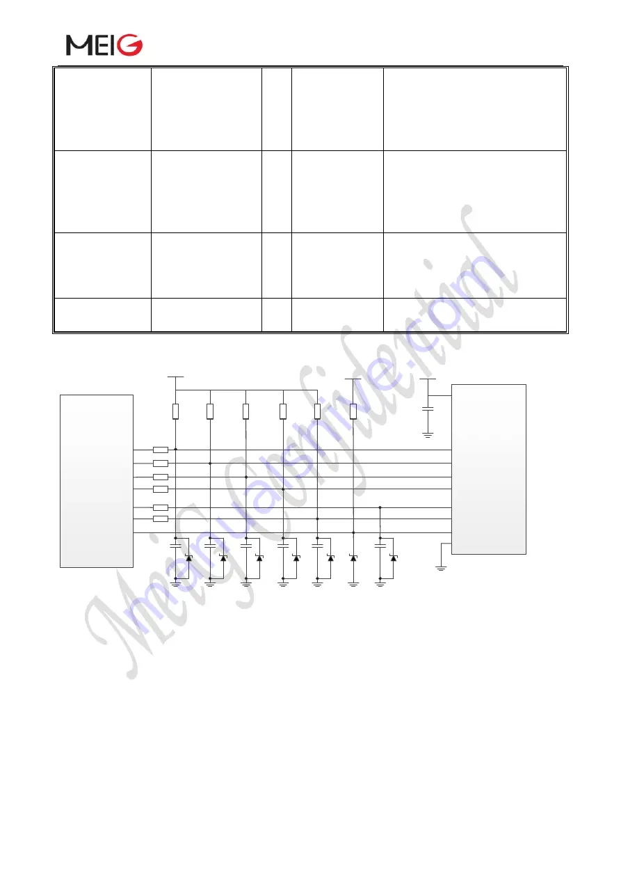
The following figure shows a reference design of SD card interface.
SD_DATA3
SD_DATA2
SD_DATA1
SD_DATA0
SD_CLK
SD_CMD
SD_INS_DET
R1 0R
R2 0R
R3 0R
R4 0R
R5 0R
R6 0R
C1
NM
D1 C2
NM
D2 C3
NM
D3 C4
NM
D4 C5
NM
D5 D7
C6
NM
D6
VDD
CD/DAT3
DAT2
DAT1
DAT0
CLK
CMD
DETECTIVE
VSS
VDD_3V
VDD_EXT
VDD_3V
SD Card Connector
C7
100nF
R7
NM
R8
NM
R9
NM
R10
NM
R11
NM
R12
470K
Module
Figure 25 Reference Circuit of SD Card Application
In the circuit design of SD card interface, in order to ensure the good performance and
reliability of SD card, the following principles are recommended in circuit design:
The voltage range of SD card power supply VDD_3V is 2.7~3.6V and a sufficient current up to
0.8A should be provided. As the maximum output current of VDD_SDIO is 50mA which can
only be used for SDIO pull-up resistors, an externally power supply is needed for SD card.
To maximally limit the surge current caused by SD card insertion, the bypass capacitor (C7) of
SD card power source should not exceed 5uF.
To avoid jitter of bus, resistors R7~R11 are needed to pull up the SDIO to VDD_SDIO. Value
of these resistors is among 10~100kohm and the recommended value is 100kohm.
In order to improve signal quality, it is recommended to add 0 ohm resistors R1~R6 in series


