


40
(1) Remove the oscillator tube (V-204) to prevent mixing at the signal generator harmonic
frequencies.
(2) Set the receiver dial to approximately 60 Mc.
(3) Set the generator to 21.4 Mc. and connect to pin 1 of V-203.
(4) Connect a high-resistance DC voltmeter (VTVM) to the cathode of the detector diode CR-
301.
(5) Set the generator output level to produce approximately 2 V on the VTVM.
(6) If the IF amplifier is known to be considerably out of adjustment, it will be necessary to
peak T-301, T-302, T-303, T-304, T-305 and T-306, to provide adequate gain.
(7) Detune the primary (T-305) counterclockwise against the stop.
(8) Increase the signal generator output to produce 2 V on the VTVM.
(9) Adjust the secondary (T-306) for maximum reading on the VTVM.
(10) Adjust the primary (T-305) for maximum reading, keeping the signal generator output
adjusted to maintain 2 V on the VTVM. DO NOT readjust the secondary (T-306) for a
maximum as this will result in improper adjustment.
(11) Repeat steps 6 through 9 for T-302, T-303 and T-304. NOTE: It is not necessary to
follow this sequence, as any transformer may be adjusted without affecting the others.
“Master” 40 Kc. IF Channel Alignment
b. 40 Kc. Band-Pass Filter. Adjustment of L-606 and L-607.— Set the function switch to
AM 40 Kc. Set the generator to 2.5 Mc. and connect to control grid of V-609. Connect the
VTVM to the grid return of V-610 and set the generator output level to approximately 2 V.
Adjust L-606 and L-607 for maximum gain.
Note: The adjustment of the L-606 and L-607 coils that form the 40-Kc. Band-Pass filter has
been carefully done at the Factory and no further attempt should normally be required.
c. 2.5 Mc. IF Amplifier.- Set the generator to 21.4 Mc. and connect to control grid of V-606.
Connect the VTVM to the to the detector diode CR-601, set the generator output level to
approximately 2 V and tune L-608, L-610 and L-611 for a maximum VTVM indication.
Eventually readjust L-606 and L-607 for a maximum indication on the Signal Strength meter
M-101 on the front panel.
Summary of Contents for G-187
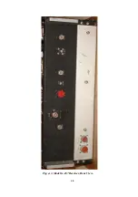
Page 7: ...7 Figure 1 1 Model G 187 Special Purpose Receiver Front View...
Page 9: ...9 Table 1 2 Semiconductor and Tube Complement...
Page 10: ...10 Table 1 2 Semiconductor and Tube Complement continued...
Page 14: ...14 Fig 2 1 Block Diagram Model G 187 Receiver...
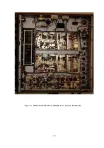
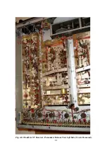
Page 44: ...44 Fig 4 1 Model G 187 Receiver Top View Cover Removed...
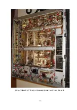
Page 45: ...45 Fig 4 2 Model G 187 Receiver Bottom View Covers Removed...
Page 46: ...46 Fig 4 3 Model G 187 Receiver Rear View...
Page 47: ...47 Fig 4 4 Model G 187 Receiver Panoramic Top View Cover Removed...
Page 48: ...48 Fig 4 5 Model G 187 Receiver Panoramic Top View Left Side Cover Removed...
Page 49: ...49 Fig 4 6 Model G 187 Receiver Panoramic Top View Right Side Cover Removed...
Page 50: ...50 Fig 4 7 Model G 187 Receiver Panoramic Bottom View Covers Removed...
Page 51: ...51 Fig 4 8 Model G 187 Receiver Panoramic Bottom View Left Side Covers Removed...
Page 52: ...52 Fig 4 9 Model G 187 Receiver Panoramic Bottom View Right Side Covers Removed...
Page 53: ...53 Table 4 2 Model G 187 Receiver Component Boards Lists...
Page 54: ...54 Fig 4 10 Model G 187 Receiver Large Component Board...
Page 56: ...56 Fig 4 14 Model G 187 Receiver Master Slave RF Tuners Top View...
Page 57: ...57 Fig 4 15 Model G 187 Receiver Master Slave Tuners Bottom View Covers Removed...
Page 58: ...58 Fig 4 16 Model G 187 Receiver Master Slave Tuners Panoramic Bottom View Covers Removed...
Page 59: ...59 Fig 4 17 Model G 187 Receiver Master RF Tuner Bottom View Cover Removed...
Page 60: ...60 Fig 4 18 Model G 187 Receiver Slave RF Tuner Bottom View Cover Removed...
Page 67: ...67 Fig 5 1 Model G 187 Receiver Schematic Diagram Master RF Tuner...
Page 68: ...68 Fig 5 2 Model G 187 Receiver Schematic Diagram Slave RF Tuner...
Page 71: ...71 Fig 5 5 Model G 187 Receiver Schematic Diagram Main Chassis Circuits...
Page 72: ...72 Fig 5 6 Model G 187 Receiver Schematic Diagram Mainframe...
Page 73: ...73 Fig 5 7 Model G 187 Receiver Schematic Diagram Power Supply Circuits...
Page 74: ...74 Fig 5 8 Model G 187 Receiver Schematic Diagram Various Details...