


19
f. OSCILLATOR BUFFER (“SLAVE” TUNER ONLY)
A 6AK5 pentode is used in this stage as “oscillator buffer”, in order to avoid any loading
effect to the oscillator itself.
3.
IF STAGES
The first 21.4 Mc IF transformers, located on the 200 Kc. IF subassembly (T-302 in the
“Master” channel and T-301 in the “Slave” channel) are connected to the respective mixer
plates through short lengths of RG-62/U coaxial cable that also carry the regulated voltage
(+150 V DC) to the mixer plates.
In addition the 21.4 Mc signal from the mixers is applied to the two channels of the
“Nuvistor” IF strip (via coaxial cables plugged into proper SMA sockets in the subchassis)
and reachs the 2.5 Mc mixer tubes (V-606/V-607 and V-601/V-602 for the “Master” and the
“Slave” channels respectively, all 6CW4’s).
The four-position “Function” switch also provides to apply the H.V. to the proper pair of IF
subchassis (200 Kc or 40 Kc IF subassemblies) depending upon the selected mode and
bandwidth.
a. FUNCTION SWITCH IN 200 Kc FM POSITION, MASTER IF CHANNEL
Two high gain stages (V-501, V-502) using 6DC6 tubes are followed by a 6CB6 (V-503) first
limiter and a 6AK5 (V-504) second limiter. A 6AL5 (V-505) is used in a discriminator circuit
of the phase-shift type. Accurate balance is obtained by using a bifilar winding for the
secondary. An automatic gain control voltage is derived from the first limiter grid circuit and
applied to the first IF amplifier stage. The first IF amplifier and the first limiter do not have
their cathode resistors bypassed, thus causing cathode degeneration which practically
eliminates the detuning caused by changes in tube input capacitance resulting from a change
in the bias voltage. Such circuitry is not necessary in the second limiter due to the different
tube structure and smaller change in grid bias. A minimum of approximately one volt bias is
on the second limiter due to grid rectification of noise signals, A self-resonant choke is
connected in the output lead of the discriminator to prevent IF signals from leaving the IF
subassembly.
Summary of Contents for G-187
Page 7: ...7 Figure 1 1 Model G 187 Special Purpose Receiver Front View...
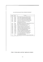
Page 9: ...9 Table 1 2 Semiconductor and Tube Complement...
Page 10: ...10 Table 1 2 Semiconductor and Tube Complement continued...
Page 14: ...14 Fig 2 1 Block Diagram Model G 187 Receiver...
Page 44: ...44 Fig 4 1 Model G 187 Receiver Top View Cover Removed...
Page 45: ...45 Fig 4 2 Model G 187 Receiver Bottom View Covers Removed...
Page 46: ...46 Fig 4 3 Model G 187 Receiver Rear View...
Page 47: ...47 Fig 4 4 Model G 187 Receiver Panoramic Top View Cover Removed...
Page 48: ...48 Fig 4 5 Model G 187 Receiver Panoramic Top View Left Side Cover Removed...
Page 49: ...49 Fig 4 6 Model G 187 Receiver Panoramic Top View Right Side Cover Removed...
Page 50: ...50 Fig 4 7 Model G 187 Receiver Panoramic Bottom View Covers Removed...
Page 51: ...51 Fig 4 8 Model G 187 Receiver Panoramic Bottom View Left Side Covers Removed...
Page 52: ...52 Fig 4 9 Model G 187 Receiver Panoramic Bottom View Right Side Covers Removed...
Page 53: ...53 Table 4 2 Model G 187 Receiver Component Boards Lists...
Page 54: ...54 Fig 4 10 Model G 187 Receiver Large Component Board...
Page 56: ...56 Fig 4 14 Model G 187 Receiver Master Slave RF Tuners Top View...
Page 57: ...57 Fig 4 15 Model G 187 Receiver Master Slave Tuners Bottom View Covers Removed...
Page 58: ...58 Fig 4 16 Model G 187 Receiver Master Slave Tuners Panoramic Bottom View Covers Removed...
Page 59: ...59 Fig 4 17 Model G 187 Receiver Master RF Tuner Bottom View Cover Removed...
Page 60: ...60 Fig 4 18 Model G 187 Receiver Slave RF Tuner Bottom View Cover Removed...
Page 67: ...67 Fig 5 1 Model G 187 Receiver Schematic Diagram Master RF Tuner...
Page 68: ...68 Fig 5 2 Model G 187 Receiver Schematic Diagram Slave RF Tuner...
Page 71: ...71 Fig 5 5 Model G 187 Receiver Schematic Diagram Main Chassis Circuits...
Page 72: ...72 Fig 5 6 Model G 187 Receiver Schematic Diagram Mainframe...
Page 73: ...73 Fig 5 7 Model G 187 Receiver Schematic Diagram Power Supply Circuits...
Page 74: ...74 Fig 5 8 Model G 187 Receiver Schematic Diagram Various Details...