


13
components mounted on a single terminal board on the underside of the main chassis.
The G-187 receiver is not intended for CW reception and so it is not equipped with a BFO.
It is also worth to say that the audio output of the G-187 receiver is at a very low level; for
sure this receiver requires an external audio amplifier associated to a good speaker for a
comfortable listening.
Figure 1-1 shows a front view of the Model G-187 receiver, and table 1-2 shows the
semiconductor and tube complement.
As shown by the various pictures of the manual, the two RF Tuners are located in the center
of the G-187 chassis, while the 200 Kc. "Double- Channel" 21.4 Mc. strip is placed near the
left side of the receiver. The 40 Kc. "Double-Channel" nuvistor 2.5 Mc. IF subchassis is
directly fastened just to the left side panel by three 1/2"-turn screws.
Near the rear panel of the unit are located the video, audio, squelch and COR circuits, while
the power supply circuits are located in the right side of the main chassis instead.
All the connections between subchassis are made by coaxial cables or color-coded single
wires.
It's also useful to notice that the components employed in the various sections of the receiver
are identified by different "prefixes" according to the section itself, i.e.:
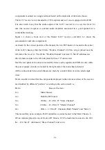
Prefix: Receiver Section:
1xx Main Chassis;
2xx Both the RF Tuners;
3xx 200 Kc. - 21.4 Mc. IF "Slave Channel"
5xx 200 Kc. - 21.4 Mc. IF "Master Channel"
6xx 40 Kc. - 2.5 Mc. IF Channels (Both "Master" and "Slave").
This means that, as an example, R-101 identifies a resistor located in the Main Chassis, L-
203 an inductor placed in one of the two RF Tuners, T-305 a trasformer located in the 200
Kc. - 21.4 Mc. IF subchassis ("Slave Channel") and so on.
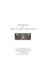
Summary of Contents for G-187
Page 7: ...7 Figure 1 1 Model G 187 Special Purpose Receiver Front View...
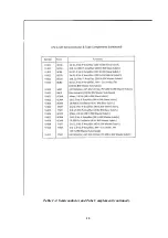
Page 9: ...9 Table 1 2 Semiconductor and Tube Complement...
Page 10: ...10 Table 1 2 Semiconductor and Tube Complement continued...
Page 14: ...14 Fig 2 1 Block Diagram Model G 187 Receiver...
Page 44: ...44 Fig 4 1 Model G 187 Receiver Top View Cover Removed...
Page 45: ...45 Fig 4 2 Model G 187 Receiver Bottom View Covers Removed...
Page 46: ...46 Fig 4 3 Model G 187 Receiver Rear View...
Page 47: ...47 Fig 4 4 Model G 187 Receiver Panoramic Top View Cover Removed...
Page 48: ...48 Fig 4 5 Model G 187 Receiver Panoramic Top View Left Side Cover Removed...
Page 49: ...49 Fig 4 6 Model G 187 Receiver Panoramic Top View Right Side Cover Removed...
Page 50: ...50 Fig 4 7 Model G 187 Receiver Panoramic Bottom View Covers Removed...
Page 51: ...51 Fig 4 8 Model G 187 Receiver Panoramic Bottom View Left Side Covers Removed...
Page 52: ...52 Fig 4 9 Model G 187 Receiver Panoramic Bottom View Right Side Covers Removed...
Page 53: ...53 Table 4 2 Model G 187 Receiver Component Boards Lists...
Page 54: ...54 Fig 4 10 Model G 187 Receiver Large Component Board...
Page 56: ...56 Fig 4 14 Model G 187 Receiver Master Slave RF Tuners Top View...
Page 57: ...57 Fig 4 15 Model G 187 Receiver Master Slave Tuners Bottom View Covers Removed...
Page 58: ...58 Fig 4 16 Model G 187 Receiver Master Slave Tuners Panoramic Bottom View Covers Removed...
Page 59: ...59 Fig 4 17 Model G 187 Receiver Master RF Tuner Bottom View Cover Removed...
Page 60: ...60 Fig 4 18 Model G 187 Receiver Slave RF Tuner Bottom View Cover Removed...
Page 67: ...67 Fig 5 1 Model G 187 Receiver Schematic Diagram Master RF Tuner...
Page 68: ...68 Fig 5 2 Model G 187 Receiver Schematic Diagram Slave RF Tuner...
Page 71: ...71 Fig 5 5 Model G 187 Receiver Schematic Diagram Main Chassis Circuits...
Page 72: ...72 Fig 5 6 Model G 187 Receiver Schematic Diagram Mainframe...
Page 73: ...73 Fig 5 7 Model G 187 Receiver Schematic Diagram Power Supply Circuits...
Page 74: ...74 Fig 5 8 Model G 187 Receiver Schematic Diagram Various Details...