17
To prevent loss of input signal due to cathode-to-filament capacity, the filaments are kept
above RF ground with broad-band chokes. The input resistance of the 416B is approximately
equal to 2/Gm when RL = RP, and in this case is 40 Ohms.
The cathode circuit is not tuned, due to the extreme bandwidth produced by the 40-Ohm shunt
load and the low cathode-to-ground capacity.
The plate tank circuit takes the form of a modified pi network and is used to couple the high
impedance plate circuit of the 416B tube to the low input impedance of the 6J4 grounded grid
second RF amplifier.
c. SECOND RF STAGE (“MASTER” OR “SLAVE” TUNER)
The output of the pi-network drives the cathode of the 6J4 grounded-grid second RF
amplifier. A low-noise second stage is used so that the system noise figure (first RF,
second RF, and mixer) is essentially that of the first stage.
The plate of the 6J4 is coupled to the grid of the 6AK5 pentode mixer by a double-tuned over-
coupled band-pass filter. A capacity "T" is used to provide coupling between the primary and
secondary tuned circuits. The shunt element of the "T" is adjustable, thus providing a control
over the interstage bandwidth.
A small iron-core inductor across the shunt element of the "T" network approaches parallel
resonance at 55 Mc, thus increasing the coupling at the low end and providing a more uniform
coupling over the tuning range of 55 to 260 Mc.
The single-tuned high Q plate circuit of the 416B tube is used to "fill in" the dip in the over-
coupled interstage network. The overall RF response when viewed at the mixer grid test point
is essentially flat over the band.
A convenient means for measuring the plate current of the 416B tube is made possible by TP-
201 at the junction of R-201 and R-202, the cathode bias resistors. A VTVM at TP-201 will
read the voltage drop across 100 Ohms. Thus 2V equals 20 mA, 5V equals 30 mA, etc.
The filament of the 416B is operated from a 12.6 volt winding of T-101 through a total series
dropping resistor of 5.1
Ohms. This produces a self-regulating effect, which extends the tube
life.
Summary of Contents for G-187
Page 7: ...7 Figure 1 1 Model G 187 Special Purpose Receiver Front View...
Page 9: ...9 Table 1 2 Semiconductor and Tube Complement...
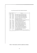
Page 10: ...10 Table 1 2 Semiconductor and Tube Complement continued...
Page 14: ...14 Fig 2 1 Block Diagram Model G 187 Receiver...
Page 44: ...44 Fig 4 1 Model G 187 Receiver Top View Cover Removed...
Page 45: ...45 Fig 4 2 Model G 187 Receiver Bottom View Covers Removed...
Page 46: ...46 Fig 4 3 Model G 187 Receiver Rear View...
Page 47: ...47 Fig 4 4 Model G 187 Receiver Panoramic Top View Cover Removed...
Page 48: ...48 Fig 4 5 Model G 187 Receiver Panoramic Top View Left Side Cover Removed...
Page 49: ...49 Fig 4 6 Model G 187 Receiver Panoramic Top View Right Side Cover Removed...
Page 50: ...50 Fig 4 7 Model G 187 Receiver Panoramic Bottom View Covers Removed...
Page 51: ...51 Fig 4 8 Model G 187 Receiver Panoramic Bottom View Left Side Covers Removed...
Page 52: ...52 Fig 4 9 Model G 187 Receiver Panoramic Bottom View Right Side Covers Removed...
Page 53: ...53 Table 4 2 Model G 187 Receiver Component Boards Lists...
Page 54: ...54 Fig 4 10 Model G 187 Receiver Large Component Board...
Page 56: ...56 Fig 4 14 Model G 187 Receiver Master Slave RF Tuners Top View...
Page 57: ...57 Fig 4 15 Model G 187 Receiver Master Slave Tuners Bottom View Covers Removed...
Page 58: ...58 Fig 4 16 Model G 187 Receiver Master Slave Tuners Panoramic Bottom View Covers Removed...
Page 59: ...59 Fig 4 17 Model G 187 Receiver Master RF Tuner Bottom View Cover Removed...
Page 60: ...60 Fig 4 18 Model G 187 Receiver Slave RF Tuner Bottom View Cover Removed...
Page 67: ...67 Fig 5 1 Model G 187 Receiver Schematic Diagram Master RF Tuner...
Page 68: ...68 Fig 5 2 Model G 187 Receiver Schematic Diagram Slave RF Tuner...
Page 71: ...71 Fig 5 5 Model G 187 Receiver Schematic Diagram Main Chassis Circuits...
Page 72: ...72 Fig 5 6 Model G 187 Receiver Schematic Diagram Mainframe...
Page 73: ...73 Fig 5 7 Model G 187 Receiver Schematic Diagram Power Supply Circuits...
Page 74: ...74 Fig 5 8 Model G 187 Receiver Schematic Diagram Various Details...

