


35
b. Mechanical Adjustments.— Normally the tuning dial will not need any adjustment in the
field, however, if the above procedure fails to restore normal operation, refer to the following:
(1) Loosen both stops of the tuning mechanism..
(2) Rotate dial to the extreme low-frequency end until the dial is stopped by the inductuner
stop of BOTH the “Master” and the “Slave” Tuners (please verify that the two inductuners
stop at the same time, if not adjust their shaft for effective stop coincidence). Hairline should
align with triangle on dial.
(3) Back up just off both the inductuner stops (for the very same amount) and tighten the set
screws in the dial drive low-frequency stop.
(4) The dial mark just below 55 Mc. should line up under the indicator (this mark is the
logging-scale "zero"). If this mark does not coincide with the indicator line, loosen the dial set
screws, align and re-tighten the screws.
(5) Rotate dial to the extreme high-frequency end until the dial is stopped by both the
inductuner stops (please verify this happens at the same time). Hairline should align with
triangle on dial, if not, loosen the screws on both the inductuner shafts and align triangle.
(6) Back up just off both the inductuner stops (for the very same amount) and tighten the set
screws in the dial-drive high-frequency stop. This completes the dial adjustments.
4. RF AMPLIFIER ALIGNMENT
(“Master” and “Slave” Tuners
).
RF Amplifier Alignment. The RF circuits are wide band compared with the IF selectivity and
are designed around the highly stable Mallory S-4 spiral inductuner. The end inductors are
also very stable, and therefore the unit should not require realignment. If realignment is found
necessary:
(1) Unsolder C-248 from the inductuner lug and solder to the BNC test connector.
(2) Connect a sweep generator with a 50-Ohm source impedance to the BNC test jack.
(3) Connect oscilloscope to front-end test point TP-202.
(4) Set the dial to 70 Mc.
(5) Adjust C-217 and C-222 for a double-tuned symmetrical response centered at 70 Mc. Use
70 Mc. marker..
Summary of Contents for G-187
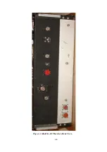
Page 7: ...7 Figure 1 1 Model G 187 Special Purpose Receiver Front View...
Page 9: ...9 Table 1 2 Semiconductor and Tube Complement...
Page 10: ...10 Table 1 2 Semiconductor and Tube Complement continued...
Page 14: ...14 Fig 2 1 Block Diagram Model G 187 Receiver...
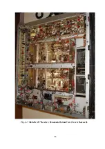
Page 44: ...44 Fig 4 1 Model G 187 Receiver Top View Cover Removed...
Page 45: ...45 Fig 4 2 Model G 187 Receiver Bottom View Covers Removed...
Page 46: ...46 Fig 4 3 Model G 187 Receiver Rear View...
Page 47: ...47 Fig 4 4 Model G 187 Receiver Panoramic Top View Cover Removed...
Page 48: ...48 Fig 4 5 Model G 187 Receiver Panoramic Top View Left Side Cover Removed...
Page 49: ...49 Fig 4 6 Model G 187 Receiver Panoramic Top View Right Side Cover Removed...
Page 50: ...50 Fig 4 7 Model G 187 Receiver Panoramic Bottom View Covers Removed...
Page 51: ...51 Fig 4 8 Model G 187 Receiver Panoramic Bottom View Left Side Covers Removed...
Page 52: ...52 Fig 4 9 Model G 187 Receiver Panoramic Bottom View Right Side Covers Removed...
Page 53: ...53 Table 4 2 Model G 187 Receiver Component Boards Lists...
Page 54: ...54 Fig 4 10 Model G 187 Receiver Large Component Board...
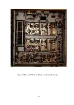
Page 56: ...56 Fig 4 14 Model G 187 Receiver Master Slave RF Tuners Top View...
Page 57: ...57 Fig 4 15 Model G 187 Receiver Master Slave Tuners Bottom View Covers Removed...
Page 58: ...58 Fig 4 16 Model G 187 Receiver Master Slave Tuners Panoramic Bottom View Covers Removed...
Page 59: ...59 Fig 4 17 Model G 187 Receiver Master RF Tuner Bottom View Cover Removed...
Page 60: ...60 Fig 4 18 Model G 187 Receiver Slave RF Tuner Bottom View Cover Removed...
Page 67: ...67 Fig 5 1 Model G 187 Receiver Schematic Diagram Master RF Tuner...
Page 68: ...68 Fig 5 2 Model G 187 Receiver Schematic Diagram Slave RF Tuner...
Page 71: ...71 Fig 5 5 Model G 187 Receiver Schematic Diagram Main Chassis Circuits...
Page 72: ...72 Fig 5 6 Model G 187 Receiver Schematic Diagram Mainframe...
Page 73: ...73 Fig 5 7 Model G 187 Receiver Schematic Diagram Power Supply Circuits...
Page 74: ...74 Fig 5 8 Model G 187 Receiver Schematic Diagram Various Details...