Linear Technology DC1974 Series Demo Manual Download Page 5

5

dc1974f

DEMO MANUAL DC1974

The DC1974 is controlled by the PScope

 System Soft-

ware provided or downloaded from the Linear Technology 

website at 

http://www.linear.com/software/

If a Kintex 7 

FPGA board and DC2159 were provided, follow the demo 

manual of these boards for proper setup.
The Kintex 7 FPGA board will act as the data collection 

board and the DC2159 is used to connect the FPGA to 

the computer. These boards both are designed to work 

seamlessly with PScope, Linear Technology’s data col-

lection software.
To start the data collection software and if “PScope.exe” 

is installed (by default) at \Program Files\LTC\PScope\, 

double click the PScope icon or bring up the run window 

under the start menu and browse to the PScope directory 

and select PScope. 
If the DC1974 is properly connected to the Kintex 7 FPGA 

board and the DC2159, PScope should automatically detect 

the DC1974 and configure itself accordingly. If necessary 

the procedure below explains how to manually configure 

PScope.
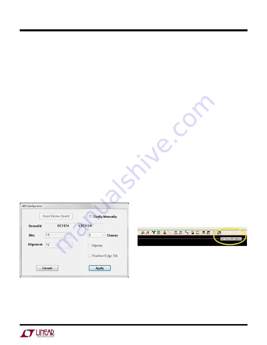
Under the “Configure” menu, go to “ADC Configuration...” 

Check the “Config Manually” box and use the following 

configuration options, shown in Figure 2:

Manual Configuration settings:
  Bits: 14
  Alignment: 16
  Channs: 2
  Bipolar: Unchecked
  Positive-Edge Clk: Unchecked
If everything is hooked up properly, powered and a suit-

able encode clock is present, clicking the “Collect” button 

should  result  in  time  and  frequency  plots  displayed  in 

the PScope window. Additional information and help for 

PScope is available in the KC705 guide and in the online 

help available within the PScope program itself.
 

NOTE:

 If a PRBS error occurs hit connect again. This 

is a bug in the first version of the software.

SERIAL PROGRAMMING

PScope  has  the  ability  to  program  the  DC1974  board 

serially through the DC2159. There are several options 

available for the LTC2124 family that are only available 

through serial programming. PScope allows all of these 

features to be tested.
These options are available by first clicking on the “Set 

Demo Bd Options” icon on the PScope toolbar (Figure 3).
This will bring up the menu shown in Figure 4.

SOFTWARE

Figure 2: ADC Configuration

Figure 3: PScope Toolbar

Summary of Contents for DC1974 Series

Page 1: ...proper input networks for dif ferent input frequencies Design files for this circuit board are available at http www linear com demo DC1974 DC1974 VARIANTS ADC PART NUMBER RESOLUTION Bit MAXIMUM SAMP...

Page 2: ...ation with the host computer Follow the instructions in Appendix A for the Xilinx KC705 based system Verilog codemaybedownloadedfromtherespectiveADClanding page www linear com LTC2123 CHANNEL 1 SINGLE...

Page 3: ...or testing purposes only In the default configuration these SMAs are not used J9 and J10 FPGA_CLK This is an optional clock input port for the FPGA It is used for testing purposes only In the default...

Page 4: ...he DC1974 is single ended there is a transformer on the board that translates the single ended signal to a differential signal to drive the ADC ANALOG INPUT NETWORK In almost all cases off board filte...

Page 5: ...configure PScope Underthe Configure menu goto ADCConfiguration Check the Config Manually box and use the following configuration options shown in Figure 2 Manual Configuration settings Bits 14 Alignm...

Page 6: ...l to the device clock or device clock twice the sample rate n Off Default DEVCLK is equal to the sample rate n On DEVCLK is twice the sample rate Overflow Enables or disables the overflow bit in the o...

Page 7: ...riods to trigger the alert in subclass 1 Valid values are 1 to 8 Alert Mode Subclass 1 Only Enables or disables the alert mode n Disabled Default Alert mode is disabled n Enabled Alert mode is enabled...

Page 8: ...chnology will need to be configured as described in the Alternate FPGA Configuration section below 4 Apply power encode clock and analog input signals to the DC1974 board 5 VerifythatPScopesoftwareisi...

Page 9: ...CONNECT DC2159 TO PC 1 ASSEMBLE BOARDS 4 POWER UP DC1974 TURN ON CLOCK AND ANALOG INPUTS 3 CONFIGURE FPGA VIA JTAG IF NECESSARY THEN REMOVE USB CABLE 2 POWER UP KC705 dc1974 F05 Figure 5 KC705 Based D...

Page 10: ...16 1 L2 IND FERRITE BEAD 33 1206 MURATA BLM31PG330SN1L 17 0 L3 RES 1206 OPT 18 2 R1 R59 RES CHIP 3 01k 1 16W 1 0402 VISHAY CRCW04023K01FKED 19 1 R2 RES CHIP 10k 1 16W 1 0402 VISHAY CRCW040210K0FKED 20...

Page 11: ...TALL 40 0 MH1 MH2 STAND OFF ALUM M3 THREAD 5 0 HEX 4 40X1 KEYSTONE 24438 DO NOT INSTALL 41 2 STENCILS STENCILS TOP BOTTOM STENCIL DC1974A 3 DC1974A A Required Circuit Components 1 1 DC1974A GENERAL BO...

Page 12: ...NTACT LINEAR TECHNOLOGY APPLICATIONS ENGINEERING FOR ASSISTANCE THIS CIRCUIT IS PROPRIETARY TO LINEAR TECHNOLOGY AND SCHEMATIC SUPPLIED FOR USE WITH LINEAR TECHNOLOGY PARTS SCALE NONE www linear com 3...

Page 13: ...E25 GND E26 HB09_P E27 HB09_N E28 GND E29 HB13_P E30 HB13_N E31 GND E32 HB21_P E33 HB21_N E34 GND E35 HB20_P E36 HB20_N E37 GND E38 VADJ E39 GND E40 SCK SCK J13A SEAM 10X40PIN J13A SEAM 10X40PIN GND...

Page 14: ...RY INCLUDING ANY WARRANTY OF MERCHANTABILITY OR FITNESS FOR ANY PARTICULAR PURPOSE EXCEPT TO THE EXTENT OF THIS INDEMNITY NEITHER PARTY SHALL BE LIABLE TO THE OTHER FOR ANY INDIRECT SPECIAL INCIDENTAL...

Reviews: