background image

3. TECHNICAL BRIEF 

- 29 -

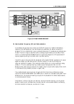
• AD6537B is an ADI designed Analog Baseband processor. AD6537B covers the processing

GMSK modulation interface, Aux ADC, Voice signal processing and Power Management.

• AD6537B consists of

1. BB Transmit section

• GMSK Modulation

• I-channel & Q-channel Transmit DACs and Filters

• Power Ramping DAC

2. BB Receive section

• I-channel & Q-channel Receive ADCs and Filters

3. Auxiliary section

• Voltage Reference

• Automatic Frequency Control DAC

• Auxiliary ADC

• Light Controllers

4. Audio Section

• 8 kHz & 16 kHz Voiceband Codec

• 48 kHz Monophonic DAC

• Power Amplifiers

5. Power Management section

• Voltage Regulators

• Battery Charger

• Battery Protection

6. Digital Processor section

• Control, Baseband, and Audio Serial Ports

• Interrupt Logic

Summary of Contents for B2070

Page 1: ...l a u n a M e c i v r e S l e d o M B2000 Service Manual B2000 P N MMBD0047201 Date March 2005 Issue 1 0 Date October 2005 Issue 1 0 Service Manual B2070 Model B2070 ...

Page 2: ...rd interface trouble 74 4 10 Earphone Trouble 76 4 11 Key Backlight Trouble 78 4 12 Receiver Trouble 80 4 13 Microphone Trouble 82 4 14 RTC Trouble 84 4 15 Indication LED Trouble 86 4 16 PTT Trouble 88 4 17 Speakerphone Trouble 89 5 DOWNLOAD AND CALIBRATION 91 5 1 Download 91 5 2 Calibration 96 6 BLOCK DIAGRAM 99 7 CIRCUIT DIAGRAM 101 8 PCB LAYOUT 106 9 ENGINEERING MODE 109 9 1 BB Test MENU 1 110 ...

Page 3: ...acturer will not be responsible for any charges that result from such unauthorized use B Incidence of Harm If a telephone company determines that the equipment provided to customer is faulty and possibly causing harm or interruption in service to the telephone network it should disconnect telephone service until repair can be done A telephone company may temporarily disconnect service as long as r...

Page 4: ...pment medical equipment etc Interference from unsuppressed engines or electric motors may cause problems H Electrostatic Sensitive Devices ATTENTION Boards which contain Electrostatic Sensitive Device ESD are indicated by the sign Following information is ESD handling Service personnel should ground themselves by using a wrist strap when exchange systemboards When repairs are made to a system boar...

Page 5: ...Bm dB relative to 1 milli watt DSP Digital Signal Processing ESD Electrostatic Discharge FPCB Flexible Printed Circuit Board GMSK Gaussian Minimum Shift Keying GPIB General Purpose Interface Bus GSM Global System for Mobile Communications IPUI International Portable User Identity IF Intermediate Frequency LCD Liquid Crystal Display LDO Low Drop Output LED Light Emitting Diode OPLL Offset Phase Loc...

Page 6: ...T Universal Asynchronous Receiver Transmitter VCO Voltage Controlled Oscillator VCTCXO Voltage Control Temperature Compensated Crystal Oscillator WAP Wireless Application Protocol SAW Surface Acoustic Wave PAM Power Amplifier Module PCB Printed Circuit Board PGA Programmable Gain Amplifier PLL Phase Locked Loop PSTN Public Switched Telephone Network RF Radio Frequency RLR Receiving Loudness Rating...

Page 7: ...Charging time Approx Under 3 75 hours RX Sensitivity GSM EGSM 104dBm DCS 104dBm TX output power GSM EGSM 33dBm Level 5 DCS PCS 30dBm Level 0 GPRS compatibility Class 10 SIM card type 3V Small Only Display Main LCD CSTN 128 x 128 pixel 65K Color Hard icons Key Pad Status Indicator 0 9 4 Menu Key Clear Key Send Key END PWR Key ANT Internal EAR Phone Jack Yes PC Synchronization Yes Speech coding EFR ...

Page 8: ... 7 2 PERFORMANCE Item Feature Comment Speaker Receiver One way dual speaker Travel Adapter Yes MP3 AAC Options Data Cable MIDI 40 Poly Mono SPK No ...

Page 9: ... 3 Frequency Error 0 1 ppm 4 Power Level Level Power Toler Level Power Toler 6 31dBm 3dB 14 15dBm 3dB 7 29dBm 3dB 15 13dBm 3dB 8 27dBm 3dB 16 11dBm 5dB 9 25dBm 3dB 17 9dBm 5dB 10 23dBm 3dB 18 7dBm 5dB 11 21dBm 3dB 19 5dBm 5dB 12 19dBm 3dB GSM EGSM EGSM 5 33dBm 2dB 13 17dBm 3dB Level Power Toler Level Power Toler 1 28dBm 3dB 9 12dBm 4dB 2 26dBm 3dB 10 10dBm 4dB 3 24dBm 3dB 11 8dBm 4dB 4 22dBm 3dB 1...

Page 10: ...3 000 6 000 5 Output RF Spectrum 6 000 due to modulation DCS PCS Offset from Carrier kHz Max dBc 100 200 250 400 600 1 200 1 200 1 800 1 800 3 000 3 000 6 000 6 000 GSM EGSM Offset from Carrier kHz Max dBm 400 600 1 200 1 800 due to switching transient 6 Output RF Spectrum 30 33 60 60 60 63 65 71 0 5 30 33 60 60 60 65 65 73 0 5 19 21 21 24 ...

Page 11: ...Level Report Accuracy 3 dB 10 SLR 8 3 dB Frequency Hz Max dB Min dB 100 12 200 0 300 0 12 11 Sending Response 1 000 0 6 2 000 4 6 3 000 4 6 3 400 4 9 4 000 0 12 RLR 2 3 dB _ _ _ 7 Spurious Emissions Conduction Emission Status due to switching DCS PCS transient Offset from Carrier kHz Max dBm 400 22 600 24 1 200 24 1 800 27 6 Output RF Spectrum ...

Page 12: ...and 1 000 Hz to be Max level in the range 14 STMR 13 5 dB 15 Stability Margin 6 dB dB to ARL dB Level Ratio dB 35 17 5 30 22 5 16 Distortion 20 30 7 10 33 3 0 33 7 7 31 7 10 25 5 17 Side Tone Distortion Three stage distortion 10 18 System Frequency 2 5 ppm 13 MHz Tolerance 19 32 768KHz Tolerance 30 ppm _ At least 65 dBspl under below conditions 20 Ringer Volume 1 Ringer set as ringer 2 Test distan...

Page 13: ... 101 dBm 0 105 dBm Battery Bar Number Voltage 0 3 36 3 58V 23 Battery Indicator 1 3 59 3 66V 2 3 67 3 73V 3 3 74V 3 87V 24 Low Voltage Warning 3 50 0 03V Standby 3 59 0 03V Call 25 Forced shut down 3 35 0 03V Voltage 1 Li ion Battery 26 Battery Type Standard Voltage 3 7V Battery full charge voltage 4 2V Capacity 780mAh Switching mode charger 27 Travel Charger Input 100 240V 50 60 Hz Output 5 2V 80...

Page 14: ...ansceiver is the integrated RF front end for multi band GSM GPRS digital cellular handsets and wireless data modems The integrated solution eliminates the IF SAW filter external low noise amplifier LNAs for three bands transmit and RF voltage controlled oscillator VCO modules and other discrete components found in conventional designs Figure 3 1 RECEIVER FUNCTIONAL BLOCK DIAGRAM H C T I W S A N N ...

Page 15: ...l the Rx and Tx paths And the input signals VC1 VC2 VC3 of a FL501 are directly connected to baseband controller to switch either Tx or Rx path on The logic and current is given below Table 3 1 Three differential input LNAs are integrated in SI4205 The GSM input supports the GSM850 869 849 MHz or E GSM 900 925 960MHz bands The DCS input supports theDCS 1800 1805 1880 MHz band The PCS input support...

Page 16: ...ters perform channel selection to remove blocking and reference interference signals The selectivity setting CSEL 0 or a low selectivity setting CSEL 1 The low selectivity filter has a flatter group channelization filter is in the baseband chip After channel selection the digital output is scaled with a digital PGA which is controlled with the DGAIN 5 0 bits in register 05h The amplified digital o...

Page 17: ...and software is able to cancel out differential DC offsets in the I Q baseband signals caused by imperfections in the D A converters The Tx Modulator implements a quadrature modulator A quadrature mixer upconverts the differential in phase TXIP TXIN and quadrature TXQP TXQN signals with the IFLO to generate a SSB IF signal that is filtered and used as the reference input to the OPLL The IFLO frequ...

Page 18: ...used for the GSM 850 and E GSM 900 bands and low side injection is used for the DCS 1800 and PCS 1900 bands The I and Q signals are automatically swapped when switching bands Additionally the SWAP bit in register 03h can be used to manually exchange the I and Qsignals Low pass filters before the OPLL phase detector reduce the harmonic content of the quadrature modulator and feedback mixer outputs ...

Page 19: ... and RF output frequencies are set by programming the N Divider registers NRF1 NRF2 and NIF Programming the N Divider register for either RF1 or RF2 automatically selects the proper VCO The output frequency of each PLL is as follows The DIV2 bit in register 31h controls a programmable divider at the XIN pin to allow either a 13 or 26 MHz reference frequency For receive mode the RF1 PLL phase detec...

Page 20: ...applications in the 824MHz to 849MHz 880MHz to 915MHz 1710MHz to 1785MHz and 1850MHz to 1910MHz bands The RF3166 incorporates RFMD s latest VBATT tracking circuit which monitors battery voltage and prevents the power control loop From reaching saturation The VBATT tracking circuit eliminates the need to monitor battery voltage thereby minimizing switching transients The RF3166 requires no external...

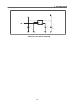
Page 21: ...or RF Circuits RF LDO U702 Two regulators are used for RF circuits One is MIC5255 U702 and the other is one port of AD6537B U101 MIC5255 U702 supplies power to transceiver SI4205 U500 One port of AD6537B supplies power to VCTCXO X500 Figure 3 6 VCTCXO CIRCUIT DIAGRAM APC X500 2V75_VVCXO 13MHz C536 22u VCC ONG OUT VCONT 100 R514 1 2 3 4 C538 1000p 15K R516 Table 3 2 RF POWER SUPPLIERS Voltage Power...

Page 22: ...3 TECHNICAL BRIEF 21 VBAT CLKON C533 10u IN U702 MIC5255 85BM5 GNO EN OUT BYP 1 2 3 4 C734 C534 RF2VBS 5 10u 0 01u 1608 Table 3 7 RF LDO CIRCUIT DIAGRAM ...

Page 23: ...Power Management U S C 32KHz CSDI CSFS CSDO BSDI BSIFS BSDO BSOFS ASDI ASDO ASFS MCLK RESET VCXOEN MCLKEN DRV OUT LNA IN RADIO AD6534 AGC Synthesizer VCO 13 26MHz JTAG VOSC AFC RAMP RF Timing I Q Interface VOICE i f Buzzer Universal System Connector USC Figure 3 8 SYSTEM INTERCONNECTION OF AD6527 EXTERNAL INTERFACE Parallel JTAG HSL GPIO Enhaoced Generic serial port A Generic serial port B Generic...

Page 24: ...t and Page Mode Flash Support for Pseudo SRAM Ciphering module for GPRS supporting GAE1 and GAE2 encryption algorithms Parallel and Serial Display Interface 8 x 8 Keypad Interface Four independent programmable backlight plus One Service Light 1 8V and 3 0V 64 kbps SIM interface Universal System Connector Interface Slow Medium and Fast IrDA transceiver interface Enhanced Generic Serial Port Dedicat...

Page 25: ...L LCD_RESET _WR 2V8_VMEM LCD_ID LCD_BL_EN Table 3 3 LCD CONTRON SIGNALS DISCRIPTION Description _LCD_CS LCD_DIM_CTRL LCD_RESET GPIO 15 _WR 2V8_VMEM LCD_ID GPIO 16 LCD_BL_EN Signals MAIN LCD driver chip enable MAIN LCD driver IC has own CS pin It controls dimming mode of LCD module GPIO_5 It determines the maker of LCD module It controls back light of LCD module GPO_23 This pin resets LCD module Th...

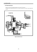
Page 26: ...F LCD BACKLIGHT LED CONTROL C RF interface The AD6527 control RF parts through PA_BAND ANT_SW1 ANT_SW2 ANT_SW2 CLKON PA_EN S_EN S_DATA S_CLK RF_PWR_DWN Signal Description PA_BAND GPO 17 PAM Band Select ANT_SW3 GPO 11 Antenna switch Band Select PA_EN GPO 16 PAM Enable Disable S_DATA GPO 20 Serial Data to PLL S_CLK GPO 21 Clock to PLL S_EN GPO 19 PLL Enable Disable RF_PWR_DWN GPO 4 Power down Input ...

Page 27: ...nds data to SIM card This model can support only 3 0 volt interface SIM card Clock 3 25MHz frequency Reset SIM block Table 3 6 SIM CONTRON SIGNALS DISCRIPTION Figure 3 9 SIM Interface of AD6527 1 2 3 7 8 4 5 6 10 9 SIM_DATA 2V85_VSIM OND1 R336 20K R337 R338 J300 VPP IO OND5 OND4 VCC RST CLK OND2 OND3 2V85_VSIM SIM_RST SIM_CLK C315 C314 NA 0 0 NA 220n 1000p C316 C317 E Key interface Include 5 colum...

Page 28: ...system supports all the GSM terminal software including the layer 1 2 and 3 of the GSM protocol stack the MMI and applications software such as data services test and maintenance It is tightly associated with on chip system SRAM and also includes boot ROM memory with a small dedicated routine to facilitate the initialization of the external Flash Memory via code download using the on chip serial i...

Page 29: ...rollers T R O P S C Ram GMSK Filter Filter Filter Filter Tone ADC ADC ADC DAC DAC ADC DAC DAC DAC T R O P S B T R O P S A h c t i w S Mic Headphones or Headset Battery Charger 8 Voltage Regulators Othello LEDs Crystal Varactor VCORE 1 8 V 80mA VMEM 1 8 or 2 8V 150mA VEXT 2 8V 170mA VSIM 1 8 or 2 85V 20mA VRTC 1 8V 200µA VABB VMIC 2 5V 1mA VVCXO 2 75V 10mA ...

Page 30: ... Transmit DACs and Filters Power Ramping DAC 2 BB Receive section I channel Q channel Receive ADCs and Filters 3 Auxiliary section Voltage Reference Automatic Frequency Control DAC Auxiliary ADC Light Controllers 4 Audio Section 8 kHz 16 kHz Voiceband Codec 48 kHz Monophonic DAC Power Amplifiers 5 Power Management section Voltage Regulators Battery Charger Battery Protection 6 Digital Processor se...

Page 31: ...DO Baseband Serial Port Control Serial Port GMSK Modulator Ramp RAM PGA PGA PGA Tx DAC Tx DAC Ramp DAC SC Filter SC Filter SC Filter Active CT Filter Active CT Filter Active CT Filter Figure 3 12 AD6537B BASEBAND TRANSMIT SECTION 3 6 2 Baseband Transmit Section 1 This section consists of two identical ADC channels that process baseband in phase I and quadrature Q input signals IP IN QP QN AD6537B ...

Page 32: ...and Voltage Reference IDAC 10 bits The Auxiliary ADC provides Two differential inputs for temperature sensing A differential input for the battery charger current sensor Figure 3 14 AD6537B AUXILIARY SECTION CSFS CSDI CSDO AD6537B Control Serial Port AFC DAC Voltage Reference REFTXCM Aux ADC AFCDAC REFBB REFOUT REF REFCHG TEMP1 TEMP2 AUXADC1 AUXADC2 AIN1P AIN2P BATTYPE ISENSE VBATSENSE LIGHT1 LIGH...

Page 33: ...o signal to speaker B2070 uses differential configuration 3 This section provides an audio codec with a digital to analog converter and an an alog to digital converter a ring tone volume controller a microphone interface and multiple analog input and output channels 4 It interconnects with external devices like main microphone main receiver and headset The descriptions of audio port used in B2070 ...

Page 34: ... AD6537B Control Serial Port CSFS CSDI CSDO 1 8V 80mA VCORE 1 8 or 2 8V 150mA VMEM VEXT 2 8V 170mA VSIM 1 8 or 2 85V 20mA 1 8V 20 A VRTC VCXOEN DBBON RESET VABB VMIC 2 5V 1mA VVCXO 2 75V 10mA VCHG GATEDRIVE BATTYPE ISENSE KEYON KEYOUT Battery Charer Didital Core LDO Regulator Regulator Control Power on Reset Generator Memory Interface LDO Regulator External Interface LDO Regulator SIM Interface LD...

Page 35: ... or 1 6V high VCORE 1 6V low VCORE 1 6V low VEXT 2 6V VCORE VMEM VEXT VSIM VVCXO 2 LDO Block 1 There are 8 LDOs in the AD6537B VCORE supplies Digital baseband Processor core and AD6537B digital core 1 8V 80mA VMEM supplies external memory and the interface to the external memory on the digitalbasebandprocessor 1 8V or 2 8V 150mA VEXT supplies Radio digital interface and high voltage interface 2 8V...

Page 36: ...in hardware 2 Charging Process Check charger is inserted or not If AD6537B detects that Charger is inserted the CC CV charging starts Exception When battery voltage is lower than 3 2V the precharge low current charge mode starts firstly And the battery voltage reach to 3 2V the CC CV charging starts 3 Pins used for charging VCHG charger supply GATEDRIVE charge DAC output ISENSE charge current sens...

Page 37: ...A E H N _ K P S _ T E S D A E H P _ C I M N _ C I M P _ C I M _ T E S D A E H N _ C I M _ T E S D A E H N _ C E R P _ C E R B 7 3 5 6 D A O T E S O L C p 9 3 0 4 1 C 3 3 1 C p 9 3 6 3 1 C p 9 3 p 9 3 3 4 1 C p 9 3 5 3 1 C A N 1 3 1 C 4 4 1 C p 9 3 9 3 1 C p 9 3 4 1 1 R 7 4 4 3 1 C p 9 3 7 4 1 1 1 R p 9 3 1 4 1 C SGND1 SGND2 R8 2 1 R _ C N 2 1 R DGND M2 2 C I P G N15 LGND 6 1 K N 3 T U O A 6 1 J P ...

Page 38: ... 0 1 R 1 2 1 0 2 E G R A H C V 6 5 3 R K 7 4 K 5 1 5 5 3 R 1 4 1 0 3 Q 0 1 1 T 9 X M I 2 5 6 3 T A B V u 1 0 4 2 3 C u 1 0 5 2 3 C 5 8 5 5 C S 2 1 0 4 Q 2 3 1 5 1 2 5 3 R 10K R357 K 1 3 5 3 R R358 10K R350 750 6 0 3 D L R359 20 T A B V E G R A H C E R P NORMAL CHARGING Trickle CHARGING Figure 3 21 CIRCUIT FOR BATTERY CHARGING AT AD6537B In order to reduce time for trickle charging additional circu...

Page 39: ... P G 8 1 A 6 3 _ O I P G 7 3 _ O I P G 6 1 C 8 3 _ O I P G 7 1 A 5 1 C 9 3 _ O I P G 4 1 K 4 _ O I P G 5 K 0 4 _ O I P G X T _ A D R I _ 0 _ O I P G 8 1 L 0 1 _ O I P G 6 1 G 1 1 _ O I P G 3 1 J 8 1 G 2 1 _ O I P G 4 1 H 3 1 _ O I P G 4 1 _ O I P G 4 1 G 5 1 _ O I P G 6 1 F 8 1 F 6 1 _ O I P G 8 1 E 7 1 _ O I P G X R _ A D R I _ 1 _ O I P G 4 1 L K L C T S R U B 4 V N I K L C 0 1 N N O K L C 3 1 P...

Page 40: ... 5 C 5 A 2 5 R E T L I F 1 6 R E T L I F 6 C 6 A 2 6 R E T L I F B1 G1 B2 G2 G3 B3 M E M V _ 8 V 2 A 6 0 3 I M E P S C 1 0 4 L F V 1 A 2 1 R E T L I F 1 1 R E T L I F 1 C 2 A 2 2 R E T L I F 1 2 R E T L I F 2 C 3 A V 1 1 R E T L I F 1 C 1 A 2 1 R E T L I F 1 2 R E T L I F 2 C 2 A 2 2 R E T L I F 1 3 R E T L I F 3 A 2 3 R E T L I F 3 C 1 4 R E T L I F 4 C 4 A 2 4 R E T L I F 5 A 2 5 R E T L I F 1 5...

Page 41: ...u 1 H n 8 1 2 0 7 L u 0 1 7 1 7 C u 1 0 6 0 7 C 8 2 7 C u 1 T X E V _ 8 V 2 u 1 9 1 7 C 7 2 7 C p 8 1 9 0 7 R K 7 4 5 1 7 C p 1 u 1 7 0 7 C H n 8 1 3 0 7 L 2 2 6 O D P 3 2 O D R 32 RFIN RFIP 31 4 2 O S S R 11 SCL SDA 13 STO 10 14 VDD 2 O L V F R V 1 S S V 7 9 X1 8 2 X L F A R F A 9 1 30 CAGC 15 CDP1 7 1 1 L P F 16 FPL2 O L G 5 GRF 29 0 2 L C C H 1 2 R C C H 27 IFADJ IFAGC 28 LIM1 25 26 LIM2 1 O L ...

Page 42: ... Y E K SP301 SP315 SP310 2 0 3 3 R 0 8 6 SP300 R L C SP313 0 8 6 0 4 3 R 0 8 6 5 3 3 R P R A H S D N E 9 8 T H G I R SP316 0 D N E S 1 8 0 3 A V 0 5 0 2 0 S 4 1 C L V A L E S 1 0 3 R K 0 1 SP309 SP304 0 5 0 2 0 S 4 1 C L V A 7 0 3 A V 6 0 3 A V 0 5 0 2 0 S 4 1 C L V A 5 P U R A T S SP317 SP306 SP303 SP312 SP311 0 8 6 2 4 3 R 0 5 0 2 0 S 4 1 C L V A 9 0 3 A V 0 8 6 9 3 3 R 0 8 6 1 4 3 R 0 5 0 2 0 S...

Page 43: ... 3 0 2 R 3 1 2 C p 9 3 p 9 3 9 0 2 C 0 0 2 2 0 M 5 L V A 0 0 2 A V p 9 3 1 0 2 C p 9 3 4 1 2 C C I M V _ 5 V 2 0 0 2 2 0 M 5 L V A 1 0 2 A V 0 1 2 C p 9 3 0 0 1 7 0 2 R 0 0 2 C I M L 3 3 C 2 4 L 5 1 4 B O 1 2 1 1 2 C u 1 0 K 2 2 4 1 2 R u 0 1 2 0 2 C N _ C I M P _ C I M 3 11 Main Speaker In the case of B2070 The main speaker is driven directly from AD6537B AOUT1P and AOUT1N pins and the gain is co...

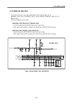
Page 44: ...K 2 2 1 0 2 R 4 0 2 R K 3 3 K 0 2 5 0 2 R 0 0 2 J T N A _ O I D A R T C E T E D _ K C A J P _ C I M _ T E S D A E H N _ T U O _ K P S _ T E S D A E H P _ T U O _ K P S _ T E S D A E H T C E T E D _ K O O H N _ C I M _ T E S D A E H Figure 3 26 HEADSET JACK INTERFACE 3 12 Headset Interface This phone chooses a 5 pin type headset which has 6 electrodes such as HEADSET_SPK_OUT_P HEADSET_MIC_P JACK_DE...

Page 45: ... 1 S B B E L 0 0 3 D L 0 2 3 C u 1 1 2 3 C u 1 8 1 3 C u 1 H 4 1 S B B E L 3 0 3 D L 4 4 3 R 7 4 1 0 3 D L H 4 1 S B B E L H 4 1 S B B E L 2 0 3 D L 2 L B _ Y E K _ I D I M 1 L B _ Y E K _ I D I M Figure 3 27 KEY BACK LIGHT ILLUMINTION 3 13 Key Back light Illumination In key back light illumination there are 6 Blue LEDs in Main Board which are driven by MIDI_KEY_BL1 and MIDI_KEY_BL2 signal from ML...

Page 46: ...E 3 D N G 2 1 N I 5 T U O u 1 0 0 2 0 3 C 5 1 3 R K 5 1 T A B V u 7 4 0 0 3 C 1SS352 D300 R399 51K 2 1 0 3 N C 1 1 0 3 C u 1 R O T A R B I V _ I D I M Figure 3 28 MOTOR 3 14 VIBRATOR The vibrator is placed in the folder cover and contacted to LCD MODULE The vibrator is driven from MIDI_VIBRATOR from ML2871HB ...

Page 47: ... 46 4 TROUBLE SHOOTING 4 TROUBLE SHOOTING 4 1 RX Trouble 13Mhz OSCILLATOR Mobile SW FEM TRANCEIVER LDO Figure 4 1 a TEST POINT ...

Page 48: ...8960 Test mode 62 CH 7 level setting TCH 62CH 60dBm setting BCCH Spectrum analyzer setting Oscilloscope setting Check regulator circuit Check VCTCXO Check FEM Mobile SW Check RX IQ Redownload SW or Do calibration again Checking Flow ...

Page 49: ... Is high Change main board NO NO YES YES Voltage at Pin5 of U702 Is 2 8V Regulator Circuit is OK See next Page to check VCTCXO Replace U702 VBAT CLKON C533 10u IN U702 MIC5255 85BM5 GNO EN OUT BYP 1 2 3 4 C734 C534 RF2V85 5 10u 0 01u 1608 Figure 4 2 1 Checking Regulator Circuit ...

Page 50: ... 7V OK No Yes Changing X500 VCTCXO Circuit is OK See next Page to check ANT SW Mobile SW Check U101 PMIC Graph 4 1 a Graph 4 1 b TEST POINT CIRCUIT Checking Flow Waveform 13 MHz O K AFC X500 2V75_VVCXO 13MHz C536 22u VCC GNO OUT VCONT 100 R514 1 2 3 1 4 C538 1000p 15K R516 2 Checking VCTCXO Circuit ...

Page 51: ... SW500 KMS 507 H n 0 1 7 1 5 C A N 0 0 5 C 2 0 5 P T 2 1 5 R 0 1 0 5 P T 7 1 5 1 X R _ S C P 2 X R _ S C P 6 1 C V 7 4 1 2 C V 3 C V 6 1 11 T N A X T _ S C P _ S C D 5 1 3 1 X R _ S C D 2 X R _ S C D 4 9 1 1 D N G 3 1 2 D N G 2 1 3 D N G 4 D N G 9 1 1 X R _ M S G 2 X R _ M S G 2 X T _ M S G 0 0 5 L F 8 5 1 A H C 7 P S M L 9 3 5 C p 0 7 2 p 0 7 2 7 3 5 C p 0 7 2 0 5 5 L H n 8 1 5 3 5 C p 2 2 3 4 5 ...

Page 52: ...d Short Yes Changing SW500 For these 2 test case No Call connection is needed No No Check RF Level of FL500 1 for GSM FL500 3 for DCS FL500 5 for PCS FEM Mobile SW is OK See next Page to check Rx IQ Signal Pin1 62dBm n 3 5 63dB No Changing FL500 Yes No For this RF Level test case RX Stand aloneMode is needed refer to chapter 11 Changing the board Table 4 2 ANT SW EGSM_Tx DCS PCS_Tx EGSM DCS_ Rx PC...

Page 53: ...aph 4 4 Similar Yes No Replace U500 TEST POINT CIRCUIT Checking Flow Waveform Graph 4 4 27 XOUT 3 N I X R P I X R 2 N Q X R 1 RXQP 28 5 N I X T 4 P I X T 7 N Q X T 6 P Q X T VDD2 32 XEN DIAG2 29 GND2 GND3 30 31 GND4 0 0 5 U 5 0 2 4 I S p 2 2 9 1 5 C 5 8 V 2 F R 2 3 5 C p 0 0 0 1 8 1 5 C u 2 2 0 0 6 1 5 C p 9 3 4 1 5 C p 9 3 N I P I N Q P Q Z H M 3 1 ...

Page 54: ... 53 4 TROUBLE SHOOTING 4 2 TX Trouble TEST POINT 13Mhz OSCILLATOR Mobile SW FEM TRANCEIVER LDO PAM ...

Page 55: ...HP8960 Test mode 62 CH 7 level setting TCH 62CH 60dBm setting BCCH Spectrum analyzer setting Oscilloscope setting Check regulator circuit Check VCTCXO Check FEM Mobile SW Check PAM contral signal Check TX IQ Redownload SW or Do calibration again ...

Page 56: ... of U702 Is 2 8V YES YES NO NO Regulator Circuit is OK See next Page to check VCTCXO Level at Pin3 of U702 Is high Replace U702 Change main board VBAT CLKON C533 10u IN U702 MIC5255 85BM5 GNO EN OUT BYP 1 2 3 4 C734 C534 RF2V85 5 10u 0 01u 1608 1 Checking Regulator Circuit ...

Page 57: ... to Graph 4 1 a Yes No No 2 7V OK Yes Changing X500 VCTCXO Circuit is OK See next Page to check ANT SW Mobile SW Check U101 PMIC TEST POINT CIRCUIT 13 MHz O K Checking Flow Waveform AFC X500 2V75_VVCXO 13MHz C536 22u VCC GNO OUT VCONT 100 R514 1 2 3 1 4 C538 1000p 15K R516 2 Checking VCTCXO Circuit ...

Page 58: ...SW500 KMS 507 H n 0 1 7 1 5 C A N 0 0 5 C 2 0 5 P T 2 1 5 R 0 1 0 5 P T 7 1 5 1 X R _ S C P 2 X R _ S C P 6 1 C V 7 4 1 2 C V 3 C V 6 1 11 T N A X T _ S C P _ S C D 5 1 3 1 X R _ S C D 2 X R _ S C D 4 9 1 1 D N G 3 1 2 D N G 2 1 3 D N G 4 D N G 9 1 1 X R _ M S G 2 X R _ M S G 2 X T _ M S G 0 0 5 L F 8 5 1 A H C 7 P S M L 9 3 5 C p 0 7 2 p 0 7 2 7 3 5 C p 0 7 2 0 5 5 L H n 8 1 5 3 5 C p 2 2 3 4 5 C...

Page 59: ... VC1 VC2 VC3 Changing board Go to 4 3 5 Checking PAM control singnal Changing SW500 Changing SW500 Pin17 29 5dBm Pin15 26 5dBm Open No No No No Yes Yes Yes Yes Short END Check RF Level of FL500 Pin 17 for GSM Pin 15 for DCS Check SW500 ANT RF with RF Cable connected Check SW500 ANT RF with RF Cable disconnected Checking Flow Check R512 R515 R517 Check whether FEM Set as TX mode Refer to Graph4 6 a...

Page 60: ...d 5 u 3 3 0 1 5 C p 2 2 9 1 5 C 12 18 GND9 7 N I _ M S G E L B A N E _ X T 3 T T A B V 4 6 P M A R V T C E L E S _ D N A N I _ S C P _ S C D 1 5 D N G 10 GND1 GND10 19 20 11 GND2 5 8 V 2 F R 2 5 8 V 2 F R 0 0 5 R K 5 1 8 1 5 C u 2 2 0 0 2 0 5 R 0 0 1 T A B V 1 0 5 C p 9 3 9 0 5 C p 0 1 5 0 5 R 0 5 1 0 5 1 4 0 5 R 6 3 3 0 5 R 6 0 5 R 0 3 0 8 1 8 0 5 R 7 0 5 R 0 8 1 p 7 2 4 0 5 C 0 0 1 1 0 5 R 1 1 5...

Page 61: ... Graph 4 8 Similar Yes No Redownload the Software And calibrate Replace U500 27 XOUT 3 N I X R P I X R 2 N Q X R 1 RXQP 28 5 N I X T 4 P I X T 7 N Q X T 6 P Q X T VDD2 32 XEN DIAG2 29 GND2 GND3 30 31 GND4 0 0 5 U 5 0 2 4 I S p 2 2 9 1 5 C 5 8 V 2 F R 2 3 5 C p 0 0 0 1 8 1 5 C u 2 2 0 0 6 1 5 C p 9 3 4 1 5 C p 9 3 N I P I N Q P Q Z H M 3 1 ...

Page 62: ... C T A B V u 2 2 7 1 1 C u 1 2 1 1 C 2V5_VMIC p 7 2 1V8_VRTC u 1 9 4 1 C 8 1 1 C K 0 1 4 0 1 R 2V8_VMEM u 1 3 1 1 C 1 P 1 E R O C V 1 N 2 E R O C V 4 A 1 T X E V 4 B 2 T X E V 3 T 1 M E M V 2 M E M V 2 T C I M V 6 1 N 7 T C T R V M I S V 6 T 6 1 D O X C V V 6 1 H B B A V T E N _ T A B V 4 T 5 1 E _ C N 5 1 E 6 1 E 6 1 E _ C N 6 1 F _ C N 6 1 F 4 3 Power On Trouble ...

Page 63: ...Does it work properly YES YES YES YES YES NO NO NO NO NO NO THE PHONE WILL POWER ON Replace the main board The power on procedure is Completed The problem may be elsewhere Does it work properly VCORE 1 8V VMEM 2 8V VEXT 2 8V VABB 2 75V WCXO 2 75V VRTC 1 8V VSIM 2 5V when sim card is inserted VMIC 2 5V Re download software Replace U101 Check the contact of power key Or dome switch Charge or Change ...

Page 64: ...G 5 E G R A H C V T A B V 2 0 8 0 1 R 7 2 1 C u 0 1 2 0 S U C 0 0 1 D G H C V 5 A 3 R L E S M E M V 8 B E S N E S T A B V 5 B _ C N 5 B 7 B _ C N 7 B 6 1 G 6 1 G _ C N 1 R 1 R _ C N 5 1 T _ C N 5 1 T 6 A E V I R D E T A G 5 T 1 T E N _ D N G E S N E S I 7 A 0 3 3 9 0 1 R R108 Q100 D100 4 4 Charging Trouble ...

Page 65: ...ge the TA Resoler the Q100 D100 R108 Replace the Q100 D100 Replace the Q100 The battery may have problems Change the battery Resolder the CN300 Pin 4 5 VCHARGE Pin 12 26 30 GND Voltage at anode of D100 5 2 V Q100 D100 R108 are well soldered Voltage across R108 is about 10 100mV 0 7 voltage R109 1 3V Battery is charged Charging is properly operating ...

Page 66: ... p 7 2 4 0 3 C 3 0 3 C u 1 1 0 4 U 5 M B 5 8 2 5 5 2 5 C I M 4 P Y B N E 3 D N G 2 1 N I 5 T U O u 1 0 0 2 0 3 C 5 1 3 R K 5 1 T A B V u 7 4 0 0 3 C 1SS352 D300 R399 51K 2 1 0 3 N C 1 1 0 3 C u 1 R O T A R B I V _ I D I M 4 5 Vibrator Trouble ...

Page 67: ...ge at pin 3 of U401 high YES YES YES YES NO NO NO NO NO NO YES YES YES Check the soldering of R315 R399 Check the soldering of C300 Check the soldering of C300 Replace U401 Replace U401 Replace vrbrator Vibrator working Resolder R315 R399 Resolder C300 Resolder C300 Is the voltage at pin 1 of U401 high Is the voltage at pin 5 of U401 high ...

Page 68: ... 67 4 TROUBLE SHOOTING TEST POINT 4 6 LCD Trouble ...

Page 69: ...CN400 Resoldering CN400 Resoldering EMI filter FL400 FL403 Reassemble FPCB with CN400 connector Replace LCD module Is the connection of FPCB with connector on PCB CN400 ok Check the soldering of EMI filter Does LCD work properly LCD working YES NO NO NO NO YES YES YES ...

Page 70: ... C 7 2 7 C p 8 1 9 0 7 R K 7 4 5 1 7 C p 1 u 1 7 0 7 C H n 8 1 3 0 7 L 2 2 6 O D P 3 2 O D R 32 RFIN RFIP 31 4 2 O S S R 11 SCL SDA 13 STO 10 14 VDD 2 O L V F R V 1 S S V 7 9 X1 8 2 X L F A R F A 9 1 30 CAGC 15 CDP1 7 1 1 L P F 16 FPL2 O L G 5 GRF 29 0 2 L C C H 1 2 R C C H 27 IFADJ IFAGC 28 LIM1 25 26 LIM2 1 O L 4 2 O L 3 N I X M 1 2 3 4 3 5 9 S N 0 0 7 U ADR 12 8 1 F p 5 2 1 _ 6 4 1 C M z H K 8 ...

Page 71: ...rom the earphone Level 1 2 8 9 pin Of U700 is OK Check U205 works properly Level 2 8 1 9 pin of U701 is OK Change U205 Change U701 Check Soldering of L202 C219 Resolder L202 C219 Change main board Check Soldering Component Around U701 OK Resolder the component Change U700 Check Soldering Component Around U700 OK Resolder the component GO to 4 10 Earphone Trouble YES YES YES YES YES YES YES YES NO ...

Page 72: ... 71 4 TROUBLE SHOOTING TEST POINT 4 8 Speaker Trouble ...

Page 73: ...2 C 5 B 1 D N G P S 3 C 2 D N G P S 3 D N G P S 4 C 5 C 4 D N G P S T U O P S 6 A T U O P S 6 B 4 A D D V P S F E R V 1 A 1 C C G E R V R W 4 F 0 D 4 E 5 F 1 D 2 D 6 F 3 D 5 E 6 E 4 D 6 D 5 D 5 D 6 D 4 D 7 D D N G D 2 B 1 B D D V D 3 D L E S F I 3 E E L I D D V O I 2 F Q R I 2 D 2 A T U O L N I X I M 3 A B H 1 7 8 2 L M 3 0 2 U 3 B T U O A 1 F K C O L C 3 F S C K 0 2 4 2 2 R 2 3 2 C u 0 1 9 N W O ...

Page 74: ...e speaker Check U202 works properly Check U206 works properly Check Voltage level of 4 5 pin of U206 Reassemble speaker Re solder U202 Re solder U206 Re solder the components Replace U203 Change main board Speaker Works properly Speaker working YES NO NO NO NO NO YES YES YES YES YES ...

Page 75: ...I S M I S V _ 5 8 V 2 A N 4 1 3 C M I S V _ 5 8 V 2 n 0 2 2 5 1 3 C 7 3 3 R 0 0 8 3 3 R 0 1 3 A 0 5 0 2 0 S 4 1 C L V K L C 3 1 D N G 4 7 2 D N G 3 D N G 8 9 4 D N G 5 D N G 0 1 6 O I 2 T S R C C V 1 P P V 5 0 0 3 J 7 1 3 C A N p 0 0 0 1 6 1 3 C 6 3 3 R K 0 2 A T A D _ M I S T S R _ M I S K L C _ M I S ...

Page 76: ...he SIM Card And try again Does it work Properly Change the SIM Card Our Phone supports only 3V SIM card Voltage at VSIM of U101 Is 3V Redownload SW Does it work Properly Replace J300 or check soldering of components Change the main board Change SIM Card SIM Card will be detected YES NO NO NO NO NO YES YES YES YES ...

Page 77: ...2 A V p 9 3 5 0 2 C T X E V _ 8 V 2 u 0 1 5 1 2 C N I V N I V 4 H u 2 2 0 0 2 L 1 0 2 U T K X E 5 7 0 9 X A M 2 D N G 1 T U O C C V 5 3 3 0 2 A V AVL5M02 200 9 1 2 C p 0 1 7 0 2 C u 0 1 K 2 2 1 0 2 R 4 0 2 R K 3 3 K 0 2 5 0 2 R 0 0 2 J T N A _ O I D A R T C E T E D _ K C A J P _ C I M _ T E S D A E H N _ T U O _ K P S _ T E S D A E H P _ T U O _ K P S _ T E S D A E H T C E T E D _ K O O H N _ C I ...

Page 78: ... mode Can you hear the sound from the earphone Voltage level check Of HEADSET_MIC_P signal Check U200 U205 works properly Voltage level check Of HEADSET_SPK_OUT_P HEADSET_SPK_OUT_N signal Resolder components Resoler U200 U205 Change main board Can you hear your voice from the earphone Can you hear your voice from the earphone Earphone will work properly Level at JACK_DETECT signal is low Resolder ...

Page 79: ... 78 4 TROUBLE SHOOTING 4 11 KEY backlight Trouble TEST POINT ...

Page 80: ...YES NO NO NO YES CIRCUIT DIAGRAM T H G I L K C A B Y E K H 4 1 S B B E L 5 0 3 D L u 1 9 1 3 C 7 4 8 4 3 R 7 4 7 4 3 R 6 4 3 R 7 4 9 4 3 R 7 4 7 4 5 4 3 R 4 0 3 D L H 4 1 S B B E L T A B V 2 2 3 C u 1 u 1 3 2 3 C H 4 1 S B B E L 0 0 3 D L 0 2 3 C u 1 1 2 3 C u 1 8 1 3 C u 1 H 4 1 S B B E L 3 0 3 D L 4 4 3 R 7 4 1 0 3 D L H 4 1 S B B E L H 4 1 S B B E L 2 0 3 D L 2 L B _ Y E K _ I D I M 1 L B _ Y E...

Page 81: ... _ K P S N _ K P S N _ C E R L E S _ K P S P _ C E R p 9 3 0 4 1 C p 9 3 3 4 1 C 4 4 1 C p 9 3 9 3 1 C p 9 3 4 1 1 R 7 4 7 4 1 1 1 R p 9 3 1 4 1 C SGND1 T8 SGND2 R8 DGND M2 2 C I P G N15 LGND 6 1 K N 3 T U O A 6 1 J P 3 T U O A AGND1 B16 AGND2 A11 5 1 K N 1 T U O A P 1 T U O A 5 1 J 9 T 1 N 2 T U O A 9 R 2 N 2 T U O A 1 1 R 1 P 2 T U O A 1 1 T 2 P 2 T U O A E N O T G N I R P _ K P S _ T E S D A E ...

Page 82: ...S or continuous wave Set the receiving volume of mobile as Max Checking Flow START Check the state of contact of dual mode speaker receiver Reassemble receiver Resolder or replace U202 Resolder R111 R114 C139 C140 C141 U202 works properly Check the voltage at 5 7 pin of U202 Change main board YES NO NO NO YES YES ...

Page 83: ...2 R 0 0 1 0 1 2 R 0 8 0 2 R K 2 2 3 0 2 R 3 1 2 C p 9 3 p 9 3 9 0 2 C 0 0 2 2 0 M 5 L V A 0 0 2 A V p 9 3 1 0 2 C p 9 3 4 1 2 C C I M V _ 5 V 2 0 0 2 2 0 M 5 L V A 1 0 2 A V 0 1 2 C p 9 3 0 0 1 7 0 2 R 0 0 2 C I M L 3 3 C 2 4 L 5 1 4 B O 1 2 1 1 2 C u 1 0 K 2 2 4 1 2 R u 0 1 2 0 2 C N _ C I M P _ C I M ...

Page 84: ... DC 2 5V Check the signal Level at each side of MIC200 mV AC Check the soldering of R207 R208 R210 C210 C211 IMicrophone will work properly Resolder component Replace microphone Resolder R200 R203 Replace U101 YES YES NO NO NO NO YES YES SETTING After intialize Agilent 8960 Test EGSM DCS mode ...

Page 85: ...N E _ A D R I N _ 2 _ O I P G 8 1 K X T _ A D R I _ 0 _ O I P G 8 1 L X R _ A D R I _ 1 _ O I P G 4 1 L N I K L C 0 1 N N O K L C 3 1 P p 0 0 0 1 9 2 1 C 2 2 1 P T R110 10M O T S _ O I D A R T C E T E D _ O I D A R L E S _ O I D A R _ K P S N O R W P N O K L C T E S E R _ 8 0 6 1 u 1 6 1 1 C u 1 5 1 1 C BAT100 u 1 4 1 1 C u 2 2 7 1 1 C u 1 2 1 1 C p 7 2 u 1 9 4 1 C 8 1 1 C K 0 1 4 0 1 R u 1 3 1 1 ...

Page 86: ...low START Is the voltage level of BAT100 1 2V Check Soldering of R104 C112 C149 Check the voltage at 1 4 of X100 Change main board Charge or change BAT100 Resolder R104 C112 C149 Resolder R110 C130 or Replace X100 YES NO NO NO YES YES ...

Page 87: ...UIT DIAGRAM 1 2 1 0 2 E G R A H C V 6 5 3 R K 7 4 K 5 1 5 5 3 R 1 4 1 0 3 Q 0 1 1 T 9 X M I 2 5 6 3 T A B V u 1 0 4 2 3 C u 1 0 5 2 3 C 5 8 5 5 C S 2 1 0 4 Q 2 3 1 5 1 2 5 3 R 10K R357 K 1 3 5 3 R R358 10K R350 750 6 0 3 D L R359 20 T A B V E G R A H C E R P Q301 Q401 ...

Page 88: ...Is about 40mV Check soldering of R350 Replace LD306 Resolder R350 Change main board Resolder Q401 Resolder Q301 Voltage level at 2pin of Q401 Is about 680mV Voltage level at 2pin of Q301 Is low YES YES YES YES NO NO NO NO Indication LED only operates in trickle charging mode ...

Page 89: ...EC_P SPK_RADIO_SEL Resolder the Cable Change the Receiver START SPKP_LDO_EN signal is High Yes No No Yes Reconnect FPCB to CN601 Connection between FPCB and CN601 is OK PTT is Operated Yes AMP_SD signal is Low Soldering between cable and board is OK Cables of Receiver are OK Only receiver is Operated Yes Yes Yes No No Yes SPK_P_SM signal is High AMP_SD signal is High ...

Page 90: ...11 C109 22u VBAT 1V8_VCORE C110 22p VBAT4 VBAT5 R4 P1 VCORE1 N1 VCORE2 T3 VMEM1 VMEM2 T2 T7 VBAT1 N2 VBAT1 1 C15 VBAT2 P2 VBAT2 1 G15 VBAT2 2 H15 VBAT3 R2 VBAT3 1 A3 VBAT3 2 B3 R5 R6 QN A14 A15 QP SPWR1 R10 SPWR2 T10 NC_R6 GND_NET2 F15 IN A13 A12 IP 5 COM GND 3 1 IN NC 4 6 NO 2 VCC U204 NLAST4599DFT2 2V8_VEXT NA R228 R226 0 NA R230 C223 0 1u REC_P RADIO_SPK_R REC_P RADIO_SPK_R SPK_RADIO_SEL ...

Page 91: ...E SHOOTING 90 Checking Flow START GO to Speaker Trouble Check R228 1 2V No Yes Replace it Check the soldering of 1 point Not OK SETTING Connect PIF to the phone and Power on Call and enter speakerphone mode OK ...

Page 92: ... 91 Figure 5 1 DOWNLOAD SETUP UART 5 DOWNLOAD AND CALIBRATION 5 1 Download A Download Setup Figure 5 1 describes Download setup 5 DOWNLOAD AND CALIBRATION ...

Page 93: ...rmes 4 Select Erase 5 Insert FDI region Don t Check OWUD 2 Press Start and Wait until Erase is completed B Download Procedure 1 Access Flash loader program in PC and select Erase Don t check OWUD 2 Press Start and Wait until Erase is completed 5 DOWNLOAD AND CALIBRATION ...

Page 94: ...1 Select Port 2 Check 3 Check 3 Press Write to start Download and press key to choose software AlchemyDate mot 5 DOWNLOAD AND CALIBRATION 93 ...

Page 95: ...ʼt Check OWUD 3 Wait until completion 4 Choose software 5 Wait until coverting from MOT to BIF is completed Donʼt check OWUD 4 Choose software 5 Wait until coverting from MOT to BIF is completed Don t check OWUD 5 DOWNLOAD AND CALIBRATION ...

Page 96: ...6 Press Start and Pover on the phone using JIG remote Power on Switch 1 5 DOWNLOAD AND CALIBRATION 95 ...

Page 97: ...Calibration Type Model Brand Wireless Communication Test Set HP 8960 Agilent RS 232 Cable and Test JIG LG RF Cable LG Power Supply HP 66311B Agilent GPIO interface card HP GPIB Agilent Calibration Final test software LG Test SIM Card PC for Software Installation Pentium II class above 300MHz 5 DOWNLOAD AND CALIBRATION ...

Page 98: ...nsfer state through the UART port LED 4 MON Indicate data transfer state through the MON port Power Source Description Power Supply Usually 4 0V Travel Adaptor Use TA name is TA 20G 24pin Switch Number Name Description Switch 1 ADI REMOTE In ON state phone is awaked It is used ADI chipset Switch 2 TI REMOTE In ON state phone is awaked It is used TI chipset Switch 3 VBAT Power is provided for phone...

Page 99: ...ate always 4 Press the Phone power key if the Remote ON is used 1st ON state D Procedure 1 Connect as Fig 6 2 RS232 serial cable is connected between COM port of PC and MON port of TEST JIG in general 2 Power ON PC then enter into Windows 98 Remark Windows 2000 system could be feasible 3 Run AUTOCAL exe the AUTOCAL application window will be appeared 5 DOWNLOAD AND CALIBRATION ...

Page 100: ...OWERKEY GATE DRIVE AOTU1 AINI AIN2 AOUT3 AOUT2 VCHG LIGHT LIGHT VOUTNOR VBAT S G D VINNOR AUXIP AUXOP1 AUXOR2 AFC Control Signal Power Audia RF ADD0 CS WR RD DIMM DATA 0 15 ADDR 0 23 ROM_CS RAM_CS 13MHz RD WD RST KEYROW 0 4 KEYCOL 0 4 POWERKEY MIDI_IRQ AUXOP2 SIM_RST CLK DATA VSIM USC 0 5 DEBUG BAT_TEMP VBAT VCHG MIDI_RST CS VSYNTHEN ANT_SW SDATA EN CLK PA_EN BAND ABB_IRQ ABB_RESET CLK_OUT MCLK_EN...

Page 101: ... Tranceiver SI4205 13MHz LDO B A S E B A N D PAM RF3166 FEM Murata VBAT DCS PCS_OUT DCS PCS_IN GSM_OUT GSM_IN GSM_IN TX_RAMP PA_EN PA_BAND 13MHz RXI RXO TXI TXQ RF_PD S_EN S_CLK S_DAT AFC 2V8_VRT ANT_SW1 ANT_SW2 VSYNTHEN 2V75_VTCXO DCS_IN PCS_IN 6 BLOCK DIAGRAM ...

Page 102: ...C119 0 068u VBAT 1u C121 OJ1 1V8_VCORE OJ3 R117 2V8_VMEM 4 7K 32 768KHz X100 MC 146_7pF 1 2 3 4 VA332 100K R131 AVLC14S02050 R130 100K C138 2V8_VEXT OJ2 1u C120 47p TP110 39p C140 0 2 R108 10u 1000p C114 C123 AVLC14S02050 VA333 C136 39p C149 27p 1u C118 10K R104 1u C115 2V75_VVCXO NA C128 TP107 C129 1000p 2V85_VSIM D100 CUS02 C103 1u R105 100 R112 82K TP114 2V85_VSIM C137 1u 4 7 R111 2V5_VMIC TP10...

Page 103: ...3 R215 4 7 C225 0 022u 10u C212 VBAT C218 39p 2V8_VEXT 39p C209 R202 C236 1u AVL5M02 200 VA200 1M C201 VA203 AVLC18S02003 39p 220K R209 4 7K R239 R201 R204 3 3K 2 2K 2 2K R214 10u C202 20K A6 SPOUT B6 A4 SPVDD VREF A1 C1 VREGC WR F4 R205 IFSEL E3 ILE IOVDD F2 IRQ D2 A2 LOUT MIXIN A3 MIXOUT B4 E1 P0_PWMA P5_VIB C6 RD E2 D1 RESET ROUT C2 B5 SPGND1 C3 SPGND2 SPGND3 C4 C5 SPGND4 SPOUT U203 ML2871HB B3...

Page 104: ...43 680 VA306 AVLC14S02050 1u 8 9 5 21 22 23 24 25 26 27 28 29 3 30 4 5 6 7 1 10 11 12 13 14 15 16 17 18 19 2 20 UP CN300 1K R353 1u C323 R399 51K LEBB S14H LD303 AVLC14S02050 VA311 SP318 SP308 R336 20K SP302 AVLC14S02050 VA305 AVLC14S02050 VA330 6 LEBB S14H LD301 SP311 680 R342 R337 0 C320 1u R350 820 3 VA310 AVLC14S02050 R326 47 VBAT VBAT R370 100 R309 680 SP305 7 CN301 1 2 C316 K1 _CE1 G8 _CE2 _...

Page 105: ...u C706 C717 10u C714 1000p A5 C5 FILTER5 2 FILTER6 1 A6 C6 FILTER6 2 B1 G1 B2 G2 G3 B3 FL401 CSPEMI306A V A1 FILTER1 1 FILTER1 2 C1 A2 FILTER2 1 FILTER2 2 C2 A3 FILTER3 1 C3 FILTER3 2 A4 FILTER4 1 FILTER4 2 C4 FILTER5 1 C2 FILTER2 2 FILTER3 1 A3 FILTER3 2 C3 FILTER4 1 A4 C4 FILTER4 2 A5 FILTER5 1 FILTER5 2 C5 A6 FILTER6 1 FILTER6 2 C6 G1 B1 G2 B2 B3 G3 CSPEMI306A FL400 V FILTER1 1 A1 C1 FILTER1 2 ...

Page 106: ...IC5255 2 85BM5 C510 33u C502 0 1p C503 RXQN 28 RXQP SCLK 13 SDI 14 SDO 11 TXIN 5 TXIP 4 TXQN 7 TXQP 6 9 VDD1 32 VDD2 XEN 26 XIN 8 XOUT 27 10 _PDN 12 _SEN GND3 GND4 31 33 GND5 GND6 34 35 GND7 GND8 36 RFIDN 19 RFIDP 18 RFIGN 21 RFIGP 20 RFIPN 17 RFIPP 16 22 RFOD 23 RFOG RXIN 3 2 RXIP 1 SI4205 U500 DIAG1 24 25 DIAG2 GND1 15 GND2 29 30 C531 C525 1 5p 1 5p C504 27p 22nH 6 2nH L506 L504 PCS_RX2 7 VC1 VC...

Page 107: ... 106 8 PCB LAYOUT Figure 8 1 B2070 BOTTOM SIDE PCB LAYOUT ...

Page 108: ... 107 8 PCB LAYOUT Figure 8 1 B2070 TOP SIDE PCB LAYOUT ...

Page 109: ... 108 ...

Page 110: ...service man engineer to view and test the basic functions provided by a handset B Access Codes The key sequence for switching the engineering mode on is 2945 Pressing END will switch back to non engineering mode operation C Key Operation Use Up and Down key to select a menu and press select key to progress the test Pressing back key will switch back to the original test menu D Engineering Mode Men...

Page 111: ...ime 3 Backlight value This controls brightness of Backlight When entering into the menu the present backlight value in the phone is displayed Use Left Right key to adjust the level of brightness The value of the brightness set at last will besaved in the NVRAM 9 1 4 Buzzer This menu is to test the melody sound 1 Melody on Melody sound is played through the speaker 2 Melody off Melody sound is off ...

Page 112: ...fault value after switching off and on the phone 1 VbControl1 VbControl1 bit Register Value Setting 2 VbControl2 VbControl2 bit Register Value Setting 3 VbControl3 VbControl3 bit Register Value Setting 4 VbControl4 VbControl4 bit Register Value Setting 5 VbControl5 VbControl5 bit Register Value Setting 6 VbControl6 VbControl6 bit Register Value Setting 9 1 9 DAI Digital Audio Interface This menu i...

Page 113: ...olume of Melody It rings in the following sequence Volume 1 Volume 2 Volume 3 Volume 0 mute Volume 4 Volume 5 9 3 4 Vibrator Vibrator is on for about 1 5 seconds 9 3 5 LCD 1 LCD Main LCD screen resolution tests horizontally and vertically one by one and fills the screen 9 3 6 Key pad When a pop up message shows Press Any Key you may press any keys including side keys but not Soft2 Key If the key i...

Page 114: ... conversation time to this 00 00 00 3 DAI DOWNLINK Speech decoder test 4 DAI OFF DAI mode off 9 6 Fact Reset MENU 6 This Factory Reset menu is to format data block in the flash memory and this procedure set up the default value in data block Attention Fact Reset i e Factory Reset should be only used during the Manufacturing process Servicemen should NOT progress this menu otherwise some of valuabl...

Page 115: ...rt select a correct COM port Baud rate 38400 Leave the rest as default values B Tx 1 Selecting Channel Select one of GSM or DCS Band and input appropriate channel 2 Selecting APC a Select either Power level or Scaling Factor b Power level Input appropriate value GSM between 5 19 or DCS between 0 15 c Scaling Factor A Ramp Factor appears on the screen You may adjust the shape of the Ramp or directl...

Page 116: ...LONE TEST 115 Figure 10 1 HW test program 10 3 Means of Test a Select a COM port b Set the values in Tx or Rx c Select band and channel d After setting them all above press connect button e Press the start button ...

Page 117: ...10 STAND ALONE TEST 116 Figure 10 2 HW test setting Figure 10 3 Ramping profile ...

Page 118: ... F Save Setting Save Current Calibration settings to setting file cal File F Load Setting Load saved Calibration setting File F Make BIN ALL Make binary file after calibration finished File F Make BIN BAT Cal only Make binary file of battery cal data only after calibration finished File F Make Write BIN Make binary file after calibration finished then download it to the Flash Memory View V Tools E...

Page 119: ...oss Enter the RF cable loss GSM and DCS Screen GPIB Primary address Enter the SS Ag8960 and PS Tektronix PS2521G GPIB address Screen ADC Channel Default ADC Calibration Channel Screen Auto Calibration Item Default Calibration Settings about Tx Rx ADC and write BIN file 118 ...

Page 120: ...ig Table and temperature Config Table 11 7 Setting check com port and cable loss Select automatic calibration item If you uncheck one item calibration will stop from the unchecked item This is useful when you want to process only oneitem 11 8 How to do calibration A Connect cable between phone and serial port of PC B Connect Ag8960 equipment and Power Supply and phone C Set correct port and baud r...

Page 121: ... 120 ...

Page 122: ... 121 12 EXPLODED VIEW REPLACEMENT PART LIST 1 2 9 3 4 26 29 28 13 20 19 18 17 27 21 16 15 24 14 12 25 11 10 23 22 8 7 5 6 12 1 Exploded View ...

Page 123: ... 122 ...

Page 124: ...PE PROTECTION MTAB0062301 Without Color 1 4 MTAD TAPE WINDOW MTAD0030601 Without Color 3 4 MTAZ TAPE MTAZ0063601 Without Color 29 3 ACGM00 COVER ASSY REAR ACGM0044201 Black 4 MCJN00 COVER REAR MCJN0030101 Black 17 4 MTAB TAPE PROTECTION MTAB0069501 Without Color 4 MTAZ00 TAPE MTAZ0063501 Without Color 27 3 AKAZ00 KEYPAD ASSY AKAZ0007509 Black 7 3 GMEY00 SCREW MACHINE BIND GMEY0004001 1 4 mm 4 0 mm...

Page 125: ...C00 TAPE SHIELD MTAC0021401 Gold 24 5 MTAC01 TAPE SHIELD MTAC0021302 3X6X0 28t meterial EMI TAPE Gold 23 5 MTAC02 TAPE SHIELD MTAC0021402 30X25X0 28t material EMI TAPE Gold 5 MTAZ00 TAPE MTAZ0060101 Without Color 22 5 MLAB00 LABEL A S MLAB0000601 HUMIDITY STICKER Without Color 5 MLAC00 LABEL BARCODE MLAC0003301 EZ LOOKS use for PCB ASSY MAIN hardware Without Color ...

Page 126: ...2 CAP CERAMIC CHIP ECCH0004904 1 uF 6 3V K X5R TC 1005 R TP 6 C103 CAP CERAMIC CHIP ECCH0004904 1 uF 6 3V K X5R TC 1005 R TP 6 C104 CAP CERAMIC CHIP ECCH0000163 47 nF 10V K X5R HD 1005 R TP 6 C105 CAP CERAMIC CHIP ECCH0004904 1 uF 6 3V K X5R TC 1005 R TP 6 C106 CAP CERAMIC CHIP ECCH0004904 1 uF 6 3V K X5R TC 1005 R TP 6 C107 CAP CERAMIC CHIP ECCH0000163 47 nF 10V K X5R HD 1005 R TP 6 C108 CAP CERA...

Page 127: ...NP0 TC 1005 R TP 6 C140 CAP CERAMIC CHIP ECCH0000120 39 pF 50V J NP0 TC 1005 R TP 6 C141 CAP CERAMIC CHIP ECCH0000120 39 pF 50V J NP0 TC 1005 R TP 6 C142 CAP CERAMIC CHIP ECCH0004904 1 uF 6 3V K X5R TC 1005 R TP 6 C143 CAP CERAMIC CHIP ECCH0000120 39 pF 50V J NP0 TC 1005 R TP 6 C144 CAP CERAMIC CHIP ECCH0000120 39 pF 50V J NP0 TC 1005 R TP 6 C149 CAP CERAMIC CHIP ECCH0000117 27 pF 50V J NP0 TC 100...

Page 128: ...004904 1 uF 6 3V K X5R TC 1005 R TP 6 C302 CAP CERAMIC CHIP ECCH0000155 10 nF 16V K X7R HD 1005 R TP 6 C303 CAP CERAMIC CHIP ECCH0004904 1 uF 6 3V K X5R TC 1005 R TP 6 C304 CAP CERAMIC CHIP ECCH0000117 27 pF 50V J NP0 TC 1005 R TP 6 C305 CAP CERAMIC CHIP ECCH0000120 39 pF 50V J NP0 TC 1005 R TP 6 C306 CAP CERAMIC CHIP ECCH0000110 10 pF 50V D NP0 TC 1005 R TP 6 C307 CAP CERAMIC CHIP ECCH0000104 3 p...

Page 129: ... D NP0 TC 1005 R TP 6 C510 CAP TANTAL CHIP MAKER ECTZ0003101 33 uF 10V M STD ETC R TP 6 C511 CAP CERAMIC CHIP ECCH0000117 27 pF 50V J NP0 TC 1005 R TP 6 C512 CAP CERAMIC CHIP ECCH0000901 2 2 pF 50V C NP0 TC 1005 R TP 6 C513 CAP CERAMIC CHIP ECCH0000178 1 8 pF 50V D NP0 TC 1005 R TP 6 C514 CAP CERAMIC CHIP ECCH0000120 39 pF 50V J NP0 TC 1005 R TP 6 C515 INDUCTOR CHIP ELCH0001003 6 8 nH J 1005 R TP ...

Page 130: ... 1 uF 10V K X5R HD 1005 R TP 6 C705 CAP CERAMIC CHIP ECCH0000182 0 1 uF 10V K X5R HD 1005 R TP 6 C706 CAP CERAMIC CHIP ECCH0000182 0 1 uF 10V K X5R HD 1005 R TP 6 C707 CAP CERAMIC CHIP ECCH0004904 1 uF 6 3V K X5R TC 1005 R TP 6 C708 CAP CERAMIC CHIP ECCH0000128 100 pF 50V J NP0 TC 1005 R TP 6 C709 CAP CERAMIC CHIP ECCH0004904 1 uF 6 3V K X5R TC 1005 R TP 6 C710 CAP TANTAL CHIP MAKER ECTZ0005201 10...

Page 131: ...0 DIODE VARIABLE CAP EDVY0001202 UFP 25 pF R TP diode capacitance C1 25 28 5pF C4 4 8 6 8pF 6 D701 DIODE VARIABLE CAP EDVY0001202 UFP 25 pF R TP diode capacitance C1 25 28 5pF C4 4 8 6 8pF 6 FL400 FILTER EMI POWER SFEY0006401 SMD 6 Channel EMI ESD CSP Pb free 6 FL401 FILTER EMI POWER SFEY0006401 SMD 6 Channel EMI ESD CSP Pb free 6 FL402 FILTER EMI POWER SFEY0006401 SMD 6 Channel EMI ESD CSP Pb fre...

Page 132: ...M ohm 1 16W J 1608 R TP 6 R111 RES CHIP ERHY0000202 4 7 ohm 1 16W J 1005 R TP 6 R112 RES CHIP ERHY0000278 82K ohm 1 16W J 1005 R TP 6 R113 RES CHIP ERHY0000280 100K ohm 1 16W J 1005 R TP 6 R114 RES CHIP ERHY0000202 4 7 ohm 1 16W J 1005 R TP 6 R117 RES CHIP ERHY0000254 4 7K ohm 1 16W J 1005 R TP 6 R118 RES CHIP ERHY0000261 10K ohm 1 16W J 1005 R TP 6 R130 RES CHIP ERHY0000280 100K ohm 1 16W J 1005 ...

Page 133: ...S CHIP ERHY0000254 4 7K ohm 1 16W J 1005 R TP 6 R242 RES CHIP ERHY0000274 51K ohm 1 16W J 1005 R TP 6 R301 RES CHIP ERHY0000261 10K ohm 1 16W J 1005 R TP 6 R304 RES CHIP ERHY0000280 100K ohm 1 16W J 1005 R TP 6 R305 RES CHIP ERHY0000280 100K ohm 1 16W J 1005 R TP 6 R306 RES CHIP ERHY0000280 100K ohm 1 16W J 1005 R TP 6 R307 RES CHIP ERHY0000280 100K ohm 1 16W J 1005 R TP 6 R308 RES CHIP ERHY000028...

Page 134: ...ES CHIP ERHY0000237 680 ohm 1 16W J 1005 R TP 6 R352 RES CHIP ERHY0007007 15 ohm 1 8W F 2012 R TP 6 R353 RES CHIP ERHY0000241 1K ohm 1 16W J 1005 R TP 6 R355 RES CHIP ERHY0000116 1 5K ohm 1 16W F 1005 R TP 6 R356 RES CHIP ERHY0000273 47K ohm 1 16W J 1005 R TP 6 R357 RES CHIP ERHY0000261 10K ohm 1 16W J 1005 R TP 6 R358 RES CHIP ERHY0000261 10K ohm 1 16W J 1005 R TP 6 R359 RES CHIP ERHY0000207 20 o...

Page 135: ...hm 1 16W J 1005 R TP 6 R707 RES CHIP ERHY0000512 10M ohm 1 16W J 1608 R TP 6 R708 RES CHIP ERHY0000201 0 ohm 1 16W J 1005 R TP 6 R709 RES CHIP ERHY0000254 4 7K ohm 1 16W J 1005 R TP 6 R710 RES CHIP ERHY0000254 4 7K ohm 1 16W J 1005 R TP 6 R711 RES CHIP ERHY0000280 100K ohm 1 16W J 1005 R TP 6 R712 RES CHIP ERHY0000241 1K ohm 1 16W J 1005 R TP 6 R713 RES CHIP ERHY0000203 10 ohm 1 16W J 1005 R TP 6 ...

Page 136: ... 3pF 1005 6 VA204 VARISTOR SEVY0004001 18 V SMD 3pF 1005 6 VA300 CAP CERAMIC CHIP ECCH0004904 1 uF 6 3V K X5R TC 1005 R TP 6 VA301 RES VARIABLE ETC ERVZ0000101 ohm PIN SMD R TP 1005 SIZE CHIP VARISTOR Pb Free 6 VA302 VARISTOR SEVY0001001 14 V SMD 50pF 1005 6 VA303 VARISTOR SEVY0001001 14 V SMD 50pF 1005 6 VA304 VARISTOR SEVY0001001 14 V SMD 50pF 1005 6 VA305 VARISTOR SEVY0001001 14 V SMD 50pF 1005...

Page 137: ... uF 6 3V K X5R TC 1005 R TP 6 C322 CAP CERAMIC CHIP ECCH0004904 1 uF 6 3V K X5R TC 1005 R TP 6 C323 CAP CERAMIC CHIP ECCH0004904 1 uF 6 3V K X5R TC 1005 R TP 6 C324 CAP CERAMIC CHIP ECCH0000182 0 1 uF 10V K X5R HD 1005 R TP 6 C400 CAP CERAMIC CHIP ECCH0004904 1 uF 6 3V K X5R TC 1005 R TP 6 C489 CAP CERAMIC CHIP ECCH0004904 1 uF 6 3V K X5R TC 1005 R TP 6 CN400 CONNECTOR BOARD TO BOARD ENBY0018701 4...

Page 138: ... CHIP ERHY0000213 47 ohm 1 16W J 1005 R TP 6 R349 RES CHIP ERHY0000213 47 ohm 1 16W J 1005 R TP 6 R350 RES CHIP ERHY0000239 820 ohm 1 16W J 1005 R TP 6 R400 RES CHIP ERHY0000274 51K ohm 1 16W J 1005 R TP 6 R401 RES CHIP ERHY0000274 51K ohm 1 16W J 1005 R TP 6 R402 RES CHIP ERHY0000274 51K ohm 1 16W J 1005 R TP 6 VA200 RES VARIABLE ETC ERVZ0000101 ohm PIN SMD R TP 1005 SIZE CHIP VARISTOR Pb Free 6 ...

Page 139: ...er Specification Color Remark 3 MHBY00 HANDSTRAP MHBY0002101 T5100 RUSSV Square Coupling Cow Leather Metal Silver 3 SBPL00 BATTERY PACK LI ION SBPL0077901 3 7 V 830 mAh 1 CELL PRISMATIC FG101 RUSSV423450 Innerpack Without Color 3 SGEY00 EAR PHONE EAR MIKE SET SGEY0003503 FG101 STERO Y TYPE 16OHM 3 SSAD00 ADAPTOR AC DC SSAD0007828 100 240V 60 Hz 5 2 V 800 mA CE CB GOST EU PLUG 24P STD ...

Reviews: