


6-1
6. LABEL AND SCREWS
6.1
6.1
6.1
6.1
OptraImage 443 Label Placement
OptraImage 443 Label Placement
OptraImage 443 Label Placement
OptraImage 443 Label Placement
6.2
6.2
6.2
6.2
Screw Classification
Screw Classification
Screw Classification
Screw Classification
6.1
6.1
6.1
6.1
OptraImage 443 Label Placement
OptraImage 443 Label Placement
OptraImage 443 Label Placement
OptraImage 443 Label Placement
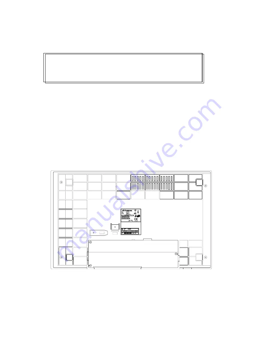
The illustration on the following page shows the location of the labels containing information that is helpful
when there is a specific problem with the unit.
The following are located on the back side of the scanner: revision label; model number, part number, &
serial number label; power & FCC label; CSA, UL, and TUV labels.
Figure 6.1 OptraImage 443 Label Placement
Figure 6.1 OptraImage 443 Label Placement
Figure 6.1 OptraImage 443 Label Placement
Figure 6.1 OptraImage 443 Label Placement
Summary of Contents for OptraImage 443
Page 1: ...OptraImage 443 Service Manual Doc No 253 0017 01 Rev 1 01 Lexmark International Inc...
Page 4: ......
Page 20: ......
Page 75: ...5 3...
Page 76: ...Lexmark Internal Use Only 5 4...
Page 77: ...5 5...
Page 78: ......


