


CrossLink-NX PCIe Bridge Board Basic Demo
User Guide
© 2021 Lattice Semiconductor Corp. All Lattice trademarks, registered trademarks, patents, and disclaimers are as listed at
All other brand or product names are trademarks or registered trademarks of their respective holders. The specifications and information herein are subject to change without notice.
10
FPGA-UG-02145-1.0
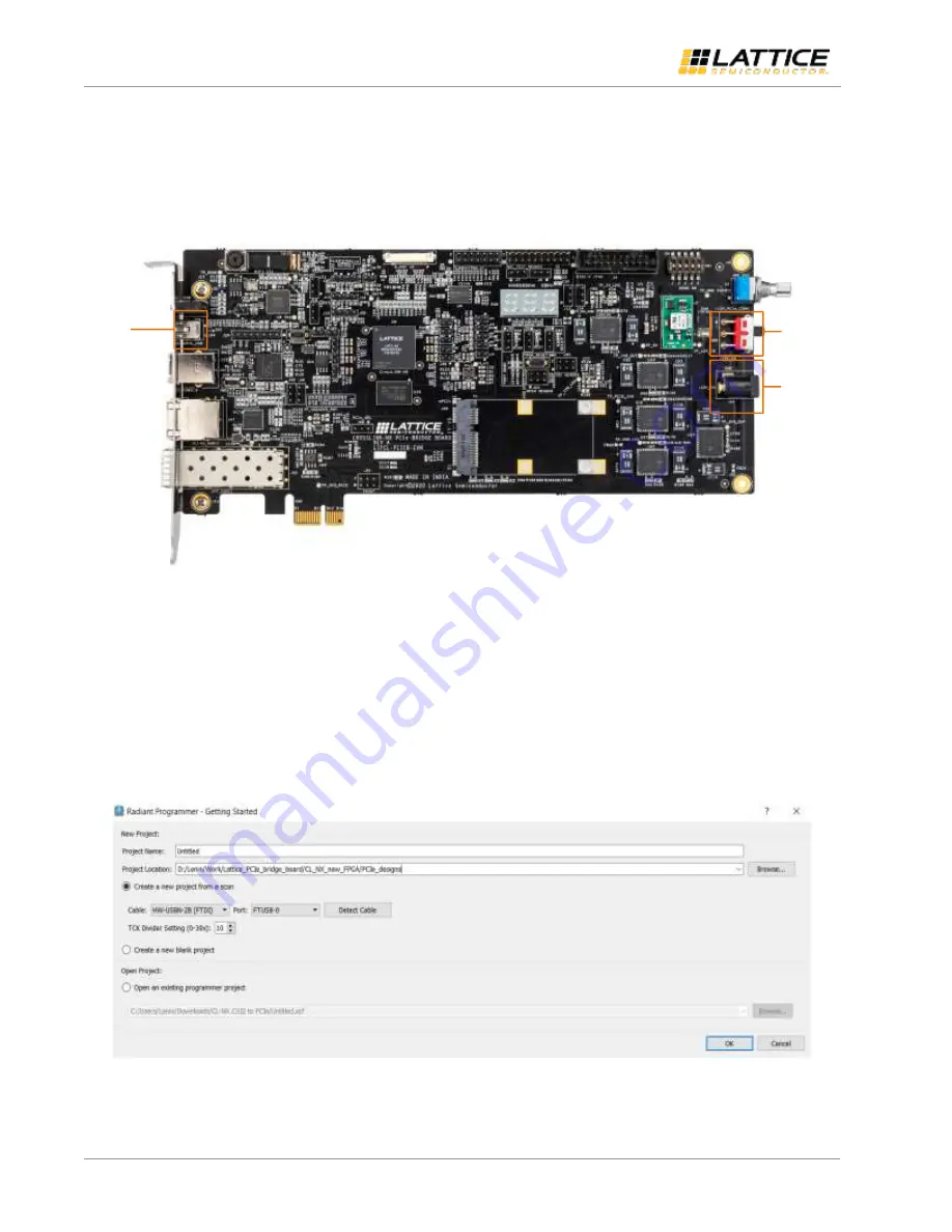
Make sure the card is plugged into a PCIe slot or connected to the 12 V input supply. If the card is plugged into the PCIe
slot, external power is provided by the system, and SW2 should be in the up position to receive power from the PCIe
slot. If external 12 V power is provided, then SW2 should be in the down position to receive power from the external
12 V connection. Connect the board to the PC running the Lattice Radiant software with the Mini USB Type A Cable as
shown in
Mini
USB
Type A
Cable
12 V Input
Supply
Connector
SW2
Figure 3.2. CrossLink-NX PCIe Bridge Board Connection
3.1.2.
Programming the FPGA
To program the CrossLink-NX FPGA device:
1.
Create a new project using the Lattice Radiant Programmer software. In the Getting Started dialog box, indicate
Project Name and Location as shown in
2.
Select Create a new project from scan. Values are indicated in the Cable, Port, and TCK Divider Setting (0-30×)
fields.
3.
Click OK.
Figure 3.3. Creating a New Project from a Scan


