COMe-bSL6 – User Guide Rev. 1.4
www.kontron.com
// 54
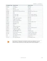
Pin
COME Signal
Description
Type
Termination
Comment
A80
GND
Power Ground
PWR GND
A81
LV
LVDS channel A clock or EDP lane 3 transmit
DP-O
Clock 20 MHz to 80 MHz
A82
LVDS_A_CK-
A83
LVDS_I2C_CK
I2C Clock for LVDS display use or eDP AUX +
I/O-3.3
PU 2.2 k
Ω
, 3.3 V
(S0)
A84
LVDS_I2C_DAT
I2C Data line for LVDS display use or eDP AUX -
I/O-3.3
PU 2.2 k
Ω
, 3.3 V
(S0)
A85
GPI3
General Purpose Input 3
I-3.3
PU 100 k
Ω
3.3 V
(S0)
A86
RSVD
Reserved for future use
NC
A87
eDP_HPD
Detection of Hot Plug / Unplug
I-3.3
PD 400 k
Ω
LVDS
/ 100 k
Ω
EDP
A88
PCIE0
Reference PCI Express clock for all PCI Express and
PCI Express graphics lanes
DP-O
100 MHz
A89
PCIE0_CK_REF-
A90
GND
Power Ground
PWR GND
A91
SPI_POWER
3.3 V power output for external SPI Flash
O-3.3
100 mA maximum
Only use to power SPI
devices on Carrier Board
A92
SPI_MISO
SPI Master IN Slave Out
(Data in to module from carrier SPI)
I-3.3
PU 15 k
Ω
to
40 k
Ω
in PCH
All SPI signals tri-stated
until reset deasserted
A93
GPO0
General Purpose Output 0
O-3.3
PD 100k
Ω
A94
SPI_CLK
SPI clock
(Clock from Module to Carrier SPI)
O-3.3
PU 15 k
Ω
to
40 k
Ω
in PCH
(S5)
All SPI signals tri-stated
with 20 K
Ω
CPU internal
weak pull-up until reset
deasserted
A95
SPI_MOSI
SPI Master Out Slave In
(Data out from Module to Carrier SPI)
O-3.3
A96
TPM_PP
TPM Physical Presence
I-3.3
PD 10k
Ω
TMP does not use this
functionality
A97
TYPE10#
Indicates to Carrier Board that type 10 Module is
installed
NC
A98
SER0_TX
Serial port 0 TXD
O-3.3
20 V protection circuit
implemented on-module,
PD on carrier boards
needed for proper
operation
A99
SER0_RX
Serial port 0 RXD
I-5T
PU 47 k
Ω
, 3.3 V
(S0)
20 V protection circuit
implemented on-module
A100
GND
Power Ground
PWR GND
A101
SER1_TX
Serial port 1 TXD
O-3.3
20 V protection circuit
implemented on-module,
PD on carrier boards
needed for proper
operation
A102
SER1_RX
Serial port 1 RXD
I-5T
PU 47 k
Ω
, 3.3 V
(S0)
20 V protection circuit
implemented on-module
A103
LID#
LID switch input
I-3.3
PU 47 K
Ω
, 3.3 V
(S5)
A104
VCC_12V
Main input voltage (4.75 V-20V)
PWR
4.75 V -
20 V
A105
VCC_12V
A106
VCC_12V
A107
VCC_12V
A108
VCC_12V
A109
VCC_12V
A110
GND
Power Ground
PWR GND
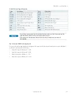
+ and -
Differential pair differentiator


