TK-5210
(
G
)
22
Q307
Ripple filter
5C
IC414
Rheostat
Q310,Q311
VCO
IC303
PLL IC
PLD
AFC
PCS_RF
SDO0
SCK0
D101
SW
IC304
1/2
IC502
DAC
X301
VCXO
IC10
ASIC
to pre-pre-drive
(Q101)
Q315
Ripple filter
15V
D210
SW
to 1st mixer
(IC202)
PCS_pot
SDO0
SCK0
Q308,Q309
IC301
ASSIST
Q312
Q306
BUFF
BUFF
IC500
VCO_MOD
TCXO_ MOD
SUM
Q314
BUFF
VCOSW1
LPF
CV
CIRCUIT DESCRIPTION
5-3. Rheostat (IC414)
The rheostat (IC414) is connected to the VCO voltage
control terminal, “V-assist”, and quickly controls the VCO
oscillation frequency. However, its accuracy is low and the
VCO frequency cannot be matched accurately with the
desired transmit carrier or the 1st local receive signal. The
rheostat is controlled by the ASIC (IC10) through the 3-lines
“PCS_pot”, “SDO0”, “SCK0” serial bus.
5-4. PLL IC (IC303)
PLL IC compares the differences in phases of the VCO
oscillation frequency and the VCXO reference frequency,
returns the difference to the VCO CV terminal and realizes
the “Phase Locked Loop” for the return control. This allows
the VCO oscillation frequency to accurately match (lock) the
desired frequency.
When the frequency is controlled by the PLL, the fre-
quency convergence time increases as the frequency dif-
ference increases when the set frequency is changed. To
supplement this, the ASIC (IC10) is used before control by
the PLL IC to bring the VCO oscillation frequency close to
the desired frequency. As a result, the VCO CV voltage does
not change and is always stable at approx. 2.0V.
The desired frequency is set for the PLL IC by the ASIC
through the 3-line “PCS_RF”, “SDO0”, “SCK0” serial bus.
Whether the PLL IC is locked or not is monitored by the
ASIC through the “PLD” signal line. If the VCO is not the
desired frequency (unlock), the “PLD” logic is low.
5-5. Local Switch (D101, D210)
The connection destination of the signal output from the
1/2 driver (IC304) is changed with the diode switch (D101)
that is controlled by the transmission power supply, 5T, and
the diode switch (D210) that is controlled by the receive
power supply, 5R.
If the 5T logic is high, it is connected to a send-side pre-
pre-drive (Q101). If the 5T logic is low, it is connected to a
receive-side mixer (IC202).
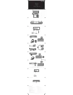
Fig. 8 PLL block diagram
6. Control Circuit
The control circuit consists of the ASIC (IC10) and its pe-
ripheral circuits. IC10 mainly performs the following;
1) Switching between transmission and reception by PTT
signal input.
2) Reading system, zone, frequency, and program data
from the memory circuit.
3) Sending frequency program data to the PLL.
4) Controlling squelch on/off by the DC voltage from the
squelch circuit.
5) Controlling the audio mute circuit by decode data input.
6-1. ASIC
The ASIC (IC10) is 32bit RISC processor, equipped with
peripheral function and ADC/DAC.
This CPU operates at 18.432MHz clock and 3.3V/1.5V
DC. It controls the fl ash memory, SRAM, DSP, the receive
circuit, the transmitter circuit, the control circuit, and the dis-
play circuit and transfers data to or from an external device.


