1-12 (No.RA033<Rev.001>)
2.6.2.4
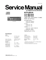
Transmitter modulation 16.8MHz PLL circuit
The transmitter modulation 16.8MHz PLL circuit produces the reference frequency signal for the Transmitter main PLL.
The circuit consists of Q301, Q302, Q303, Q304, Q305, X301, IC301, IC302 and IC303.
19.2MHz reference signal is amplified by Q402 and is fed to IC301 as a PLL reference signal.
VCXO of X301 generates 16.8MHz signal. The signal enters buffer amp Q305. Then it is amplified by Q304 to feed PLL IC of IC301.
Also, the signal is fed to TX main PLL of IC104.
PLL IC of IC301 compares the phase between the 16.8MHz signal and the reference 19.2MHz signal. The phase error will be filtered
as a DC signal and the DC signal controls the frequency of X301.
The modulation 16.8MHz PLL's loop bandwidth is very small (less than 5Hz). The modulation signal is added by IC302 to phase error
filter output.
The controlled DC voltage is fed to IC303 operational amplifier from C317 and C320, and the output signal (MOD_CV) is monitored
by AD converter IC of IC804.
PLL's lock and unlock state is monitored by Q301 and Q302 as a signal name "MOD_UL".
Fig.4 Transmitter Modulation 16.8MHz PLL circuit
2.6.2.5
Transmitter main PLL circuit
The transmitter main PLL circuit consists of the VCO (D103, D104, D105, D106, D107, D108, D109, D110, D111, D112, D113, Q101,
Q102, Q105, Q106, Q107, Q108, Q109, IC101, IC102 and IC103) and PLL (Q103, Q110 and IC104). They produce the transmitter
frequency signal.
If VCO_A/B signal is high, Q105 is activated and the VCO Q107 produces transmitter frequencies from 136.000MHz to 154.995MHz.
If VCO_A/B signal is low, Q106 is activated and the VCO Q108 produces transmitter frequencies from 155.000MHz to 174.000MHz.
VCO oscillation frequency is controlled by TXASSIST signal mainly. The DC signal of TXASSIST is proportional to TX frequency.
The signal produced by the VCO (Q107 or Q108) is amplified by Q109. The signal is divided to PLL multiplier amplifier and driver
amplifiers by a power divider circuit (L135, L136, C192 and R181).
PLL multiplier amplifier Q110 is multiply the VCO signal and feed the signal to IC104.
PLL IC of IC104 compares the phase between the multiplying of VCO signal and the reference 16.8MHz modulated signal. The phase
error will be filtered as a DC signal and the DC signal controls the frequency of VCO.
PLL control voltage is constant value (2.9 to 3.1V) because the TXASSIST signal adjusts the VCO frequency roughly.
The controlled DC voltage is fed to IC103 operational amplifier, and the output signal (TX_CV) is monitored by AD converter IC of
control unit (XC1-064).
PLL's lock and unlock state is monitored by Q103 as a signal name "TX_UL".
Fig.5 Transmitter main PLL circuit
Internal Freq.
Ref 19.2MHz
PLL circuit
19.2MHz
MOD 16.8MHz
PLL IC
33C
VCXO
16.8MHz
33C
Op-Amp
50C
MOD_CV
50C
50C
TX main
PLL circuit
16.8MHz
16.8MHz
IC301
IC303
X301
Q305
Q304
33C
IC302
VCXO MOD
8
2
6
TX Mod
16.8MHz
PLL circuit
16.8MHz
TX main PLL
33C
Op-Amp
50C
TX_CV
33C
50C
Driver
circuit
136
174MHz
IC104
IC103
IC101
Q110
X2
ATT
50C
200C
Ripple
Fil
Q101
TXASSIST
VCO_MOD
Ripple
Fil
SW
SW
80C
VCO-B
Q108
Q106
Q105
VCO-A
Q107
Q102
VCO_A/B
IC102
Q109
9
2
6
Summary of Contents for NXR-5700
Page 121: ...MEMO ...