NXR-901
10
CIRCUIT DESCRIPTION
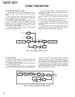
2-4. Transmitter main PLL circuit
The transmitter main PLL circuit consists of the VCO (Q4)
and PLL IC (IC5). They produce the transmitter frequency
signal.
The VCO Q4 produces transmitter frequencies from
467.5~470.5MHz. The VCO’s tuning voltage is adjusted by
buffer amplifi er IC6 and DAC IC201 pin 1.
The VCO frequency tuning voltage is adjusted by the
IC201 pin 1 DAC signal, the IC6 DC amplifi er and the low
pass fi lter. The LPF is confi gured with R28, C39 and D1. The
VCO frequency tuning voltage is monitored by the IC3 DC
buffer and the IC703 pin 16 ADC.
The signal produced by the VCO (Q4) is fed to the buffer
amplifi er and is amplifi ed by Q6.
The VCO signal is doubled by Q5 to 935~941MHz. This
signal is fed to the BPF to attenuate spurious signals, and is
then fed to PLL IC (C5).
The phase difference signal produced by the comparing
phase is converted to a DC voltage by a lag-lead type loop
fi lter.
The DC signal is applied to varicaps D2 and D3 to lock
the VCO oscillator with the desired oscillator frequency.
At the same time, the DC signal passes through the IC3
operational amplifi er for monitoring the transmitter main PLL
lock voltage.
The output from the VCO passes through frequency
doubler Q8 and Q9. The produced 900MHz band signal is
fi ltered by the BPF to attenuate spurious signals.
Fig. 3 Transmitter main PLL circuit
Q6
Q4
BPF
ATT
Q5
PLL IC
Power
divider
Freq. doubler and
driver amplifiers
IC5
BUFF
IC3
BUFF
IC6
CV_ADJ2
CVT
TX Mod 1
9
.2MHz
PLL circuit
467.5~470.5MHz
9
35~
9
41MHz
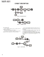
2-5. Driver circuit
The driver circuits consist of a frequency doubler circuit
(VCO’s 467.5~470.5MHz signal is doubled to 935~941MHz)
and a transmitter driver amplifi er.
The frequency doubler consists of Q8 and Q9. Spurious
signals are fi ltered by the BPF.
The driver amplifi ers consist of Q10, Q11 and SAW band-
pass filter L34. The Driver output power is levelled by D7
and IC8 to adjust Q11’s Vg voltage (to control Vg, Id will be
changed; to change Id, gm will be changed; then, the gain of
Q11 is changed). The output power of CN802 is 16dBm and
is to be adjusted with a 50
termination. L34 is an additional
SAW band-pass fi lter. The SAW fi lter reduces the frequency
doubler's spurious signals. In addition, the SAW fi lter attenu-
ates broadband noise from the VCO, doubler and buffer am-
plifi ers on the GPS downlink band.
Fig. 4 Frequency doubler and driver circuit
IC8
A/2
IC8
B/2
BPF
BPF
(SAW)
Q10
Q11
Q8,Q
9
9
35~
9
41MHz
L34
467.5~470.5MHz
Doubler
TX main
PLL circuit
DET
LPF
D7
D_PC
TX UNIT
CN802
TX_OUT
+16dBm
Summary of Contents for NEXEDGE NXR-901
Page 154: ...1 E CN300 RX_IF_VN ...

