NXR-901
18
CIRCUIT DESCRIPTION
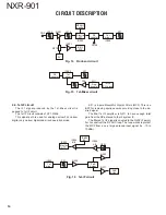
5. Baseband Signal Processing Part
The baseband circuit is located on the Control unit (X53-
413).
This circuit enables the selection of the Analog Signal
Processing mode and the Digital Signal Processing mode,
and adjusts the level of the baseband signals in each mode.
This circuit consists of IC2, IC3, IC5, IC8, IC9, IC12,
IC14, IC19, IC20 and IC21.
The type of input modulation signals are local micro-
phone terminal, low-speed data (LSD), high-speed data
(HSD), external audio input (TA), and external data input (TD),
and also the type of output demodulation signals are receiv-
ing audio output (RA), and receiving data output (RD).
The multiplexer (IC2, IC3, IC14) selects the signal path,
the electronic volume (IC8) adjusts the signal level, and the
operational amplifi ers (IC5, IC9, IC12, IC19, IC20, and IC21)
amplify and sum various signals.
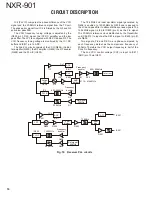
5-1. Demodulation circuit
(Analog/Digital signal processing)
In case of the Analog Signal Processing mode, the de-
tected audio signal obtained from the IF SYSTEM IC (X55-
312 IC207) is amplifi ed by IC5 (A/2), input into the AINR ter-
minal of CODEC IC (IC4), and then processed as an audio
signal by the DSP (IC37).
The processed audio signal from the AOUTR terminal
of IC4 is amplifi ed to a suffi cient level by IC12 (A/2), and is
then passed through the anti-aliasing fi lter at IC12 (B/2).
In case of the Digital Signal Processing mode, the detect-
ed audio/data signal obtained from the IF SYSTEM IC (X55-
312 IC501) is input into the ADC (X53-414 IC312).
Receiving signal processing is performed by RX_DSP
(X53-414 IC323), and voice decode processing is performed
by TX_VOCODER DSP (X53-414 IC324).
The processed audio signal from the AOUTL terminal of
the CODEC IC (X53-414 IC309) is amplifi ed to a suffi cient
level by IC20 (D/4), and is then passed through the anti-
aliasing fi lter at IC20 (C/4).
The audio signal path is selected by the multiplexer (IC14)
depending on the Analog mode (IC14 is setting Y=Y0) or the
Digital mode (IC14 is setting Y=Y1).
The audio signal is then routed through an electronic
volume (IC8) V3/V4 to the multiplexer IC (IC25), and is am-
plifi ed to a suffi cient level to drive the loudspeaker using an
audio power amplifi er (IC29).
5-2. Audio amplifi er circuit
The audio amplifi er circuit is located in the control section
of the Control unit (X53-413).
The 3W output audio power is available from the pin 15
test connector “SPO, SPG” on the rear panel to the external
speaker, in the case of a 13.8V power supply voltage and 4
ohm load.
5-3. Microphone circuit
The signal from the microphone is passed through the
AGC circuit located in the DISPLAY circuit (X56-315 B/3) so
that it may not saturate.
This circuit consists of IC926, D933, D934 Q931, and
Q932.
The AGC controls the amplifi er gains using the detected
audio signal depending on the positive and negative peaks
of the signal amplitude.
The audio signal goes to the control section of the Con-
trol unit (X53-413) from the DISPLAY circuit (X56-315 B/3).
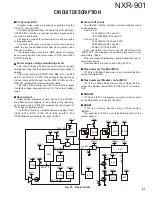
5-4. Modulation circuit
(Analog/Digital signal processing)
The transmitting audio signal goes to the input terminal
of the multiplexer IC (IC3) for microphone muting.
In case of the Analog Signal Processing mode (multiplexer
IC3 is setting X=X0), the audio signal is amplifi ed by IC9 (A/4),
input to the AINL terminal of the CODEC IC (IC4), and audio
processed by the DSP (IC37).
The processed audio signal from the AOUTL terminal of
IC4 is amplifi ed to a suffi cient level by IC9 (B/4), and is then
passed through an anti-aliasing fi lter at IC9 (C/4), and ampli-
fi ed by the summing (TD) amplifi er IC9 (D/4).
On the other hand, in the case of the Digital Signal Pro-
cessing mode (multiplexer IC3 is setting X=X1), the audio
signal is amplifi ed by IC20 (A/4), input to the AINL terminal
of the CODEC IC (X53-414 IC309), and processed by the
TX_VOCODER DSP (X53-414 IC324).
The processed audio signal from the AOUTR terminal of
IC309 passes through the anti-aliasing fi lter at IC19 (B/2).
6. Control Circuit
The control circuit consists of two units, X53-413 and
X53-414.
Unit X53-413 mainly has the power supply circuit, base-
band signal path selection circuit (level adjustment is in-
cluded), analog mode voice codec circuit, and RF controller
circuit.
Unit X53-414 has the mode selection (analog or digital)
circuit, digital mode communication processing circuit, LAN
interface circuit, and Compact Flash interface circuit.
6-1. X53-413
■
RF control MPU
The IC34 RF control MPU is a 16-bit single chip micro-
processor incorporating 256K bytes of ROM and 20K bytes
of RAM.
This MPU controls the Flash memory, DSP, Receiver unit,
Transmitter unit, the EEPROM of each unit, and the display
circuit, and has communication I/F with external devices.
■
DSP
The DSP circuit is in charge of the fi ltering of transmitting
and receiving signals, and the encoding and decoding of
sub-audible signals (encode: QT, DQT, DTMF, decode: QT,
DQT, DTMF).
This circuit consists of IC37, IC30, IC31, IC4, IC5, IC9,
and IC12.
The receiving signal, DET is converted from analog to
digital by IC4 with a sampling frequency of 16.128kHz.
The digitized audio signal is sent to the DSP (IC37) to
process the sub-audible signal and audio signal. The pro-
cessed digital audio signal is applied to CODEC IC4, and is
converted from digital to analog.
Summary of Contents for NEXEDGE NXR-901
Page 154: ...1 E CN300 RX_IF_VN ...


