NXR-901
9
CIRCUIT DESCRIPTION
reference signal, the 5.99MHz internal DDS (IC401) is se-
lected as the reference signal.
If the OCXO unit is installed and there is no external
reference signal, the 10MHz OCXO unit is selected as the
reference signal.
If an external reference signal (CN408/ 10MHz/ 0dBm or
higher/ Zin=50
) is applied, the external reference signal is
selected as the reference signal irrespective of an existing
OCXO unit.
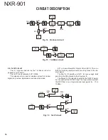
The internal/external reference circuit consists of D401,
D402, D503, D507, D509, D510, D516, D517, D518, D519,
Q403, Q404, Q501, Q502, Q507, Q508, Q509 and Q510.
The DDS circuit consists of X401, IC401, IC402, IC403,
CF401, Q401 and Q402.
In any conditions, the “REF OUT” terminal provides a
10.0MHz reference signal (CN403/ 10.0MHz/ more than
+5dBm/ Zload=50
). The “REF OUT” frequency accuracy is
dependant on the internal reference TCXO X401, optional
internal OCXO unit, KXK-3 (M3) or “REF IN” signal.
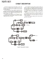
2-2. Internal frequency reference 20.0MHz PLL
circuit and 1/2 divider
The internal reference 20.0MHz PLL circuit produces a
reference frequency signal for the transmitter modulation
19.2MHz PLL circuit, the Receiver unit (X55-312) 1st/2nd
PLL IC and the Control unit (X53-414) DSP’s clock PLL IC.
This circuit consists of Q307, Q306, Q308, Q309, X301,
IC302 and IC303.
The 5.99MHz or 10MHz signal produced by the internal/
external reference circuit is amplifi ed by IC301 and supplied
to the PLL IC (IC303) reference signal pin.
The VCXO (X301) signal enters buffer amplifier Q307
and is amplifi ed by Q306. The higher harmonic wave is at-
tenuated by LPF and returns to IC303. Its phase is com-
pared with that of the reference frequency 10kHz.
The phase difference signal produced by the comparing
phase is converted to a DC voltage by a lag-lead type loop
fi lter.
This DC voltage is input to the X301 control voltage ter-
minal for controlling the VCXO oscillating frequency.
The DC voltage passes through the IC302 operational
amplifier, and is output as a voltage signal (CVT-REF) for
monitoring the reference 20.0MHz PLL circuit lock voltage.
The stabilized 20.0MHz reference oscillating signal en-
ters the Q308 and Q309 buffer amplifi ers and is amplifi ed by
Q310 and Q311.
The higher harmonic wave is attenuated by the LPF, fed
to IC205 and used as the reference frequency signal for the
transmitter modulation 19.2MHz PLL circuit.
The phase locked 20.0MHz signal is also used as the
reference signal for the Receiver unit (X55-312) and Control
unit (X53-414). Q310 is the buffer amplifi er to Control unit,
and it is connected to CN405. Q311 is the buffer amplifi er for
the Receiver unit, and is connected to CN406.
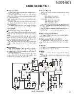
There is a 1/2 divider circuit consisting of Q503, Q506,
Q514, IC503, IC504, IC501. The 20.0MHz signal from Q308
is fed to Q514 and IC504 buffer amplifiers to amplify the
necessary level. IC503 divides the input signal to be half the
frequency. The 10.0MHz signal is levelled by the AGC circuit
of Q503 and Q506 to meet a wide range of load impedance.
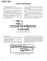
2-3. Transmitter modulation 19.2MHz PLL circuit
The transmitter modulation 19.2MHz PLL circuit pro-
duces the reference frequency signal for the main PLL and
modulates the low-frequency components.
The circuit consists of X201, IC204, IC205, IC206, IC208,
Q3, Q205 and Q206. The signal generated by the VCXO
(X201) is fed to the buffer amplifi er Q206 and is amplifi ed by
Q205 to feed the PLL IC (IC204).
The 20.0MHz reference signal is fed by IC205. Its phase
is compared with that of the 5kHz reference frequency.
The phase difference signal produced by the comparing
phase is converted to a DC voltage by a lag-lead type loop
fi lter.
This DC voltage is input to the IC206 invert amplifi er (B/2)
and is synthesized with the modulating signal.
This DC voltage is input to the X201 control voltage ter-
minal for controlling the 19.2 MHz VCXO oscillating frequen-
cy.
The DC voltage passes through the IC208 operational
amplifi er, and is output as a voltage signal (CVT_MOD) for
monitoring the modulating 19.2MHz PLL circuit lock voltage.
The 19.2MHz signal is buffered by Q3. The higher har-
monic wave is attenuated by the LPF, fed to IC5, and is used
as the reference frequency signal of the transmitter main
PLL circuit.
Q206
X201
Q3
TX unit
Q30
9
TX unit
IC5
LPF
BUFF
IC205
PLL IC
IC204
BUFF
IC208
LPF
LPF
20.0MHz
Q205
IC206
B/2
CVT_MOD
1
9
.2MHz
Mod signal
Fig. 2 Transmitter modulation 19.2MHz PLL circuit
Summary of Contents for NEXEDGE NXR-901
Page 154: ...1 E CN300 RX_IF_VN ...

